AMD Geode SC2200 Processor Data Book
Publication ID 32580B
Contacts Trademarks
Advanced Micro Devices, Inc. All rights reserved
Contents
Video Processor Module
Electrical Specifications
Package Specifications
Core Logic Module
ACCESS.bus Data Transaction
Power Supply Connections
Typical Battery Configuration
Typical Battery Current Normal Operation Mode
325
Multiword DMA Data Transfer Timing Diagram 411
Fast IR MIR and FIR Timing Diagram 428
Enhanced Parallel Port Timing Diagram 430
434
431
432
433
32580B
RTC Configuration Registers
SIO Control and Configuration Register Map
SIO Control and Configuration Registers
Relevant RTC Configuration Registers
174
124
Banks 0 and 1 Common Control and Status Registers 125
126
F3 PCI Header Registers for Audio Configuration
Pciusb USB PCI Configuration Register Summary
F0BAR0+I/O Offset Gpio Configuration Registers
F2BAR4+I/O Offset IDE Controller Configuration Registers
PLL3
SuperI/O
General Description
Video Processor
Core Logic
Video Processor Module
Features
General Features
GX1 Processor Module
Overview
Other Features
Nand Eeprom
SuperI/O Module
32580B
Architecture Overview 32580B
GX1 Module
Memory Controller
Video Processor Module
SC2200 Memory Controller Registers
Width Memory Offset Bits Type Name/Function Reset Value
SC2200 Memory Controller Register Summary
MCMEMCNTRL2 R/W
Rsvd Reserved. Write as GXBASE+840Ch-840Fh
Bit Description GXBASE+8408h-840Bh
Mcbankcfg R/W
Rsvd Reserved. Write as 0070h
Mcdracc R/W
Mcgbaseadd R/W
Mcdradd R/W
Video Input Port
Fast-PCI Bus
Display
1 GX1 Module Interface
Other Interfaces of the Core Logic Module
System Reset
Clock, Timers, and Reset Logic
Reset Logic
Power-On Reset
SC2200
Signal Definitions 32580B
CRT Interface IDE/TFT Interface
AMD Geode
Jtag Interface
USB
Mnemonic Definition
Signal Definitions Legend
Ball Assignments
AMD Geode
BGU481 Ball Assignment Sorted by Ball Number
Configuration
RD#
Slct
Buffer1 Power Signal Name
VPD7
AD8 Inpci
PWR AD0 Inpci
AA4 IDEDATA5
MA9
AL8 SDATAIN2
Signal Name Ball No
BGU481 Ball Assignment Sorted Alphabetically by Signal Name
C30
FC/BE3# C17
U31
B20
MD29 AD29
MD27 AC30
MD28 AE31
C11
J28
F31
J30
J29
Strap Options
Nominal External PU/PD Strap Settings
Strap Options
TFT, CRT, PCI, GPIO, System
Multiplexing Configuration
Two-Signal/Group Multiplexing
Default Alternate Ball No Signal Configuration
AC97 Fpci Monitoring
ACCESS.bus
Internal Test
Three-Signal/Group Multiplexing
Fpvddon
Four-Signal/Group Multiplexing
Gxclk
TEST3
Boot ROM is 16 Bits Wide. This strap signal enables
Signal Descriptions
Signal Name Ball No Type Description Mux
Maximum Core Clock Multiplier. These strap signals
AH2
AJ2
AJ3
AG3
Column Address Strobe. RAS#, CAS#, WE# and CKE
Memory Interface Signals
Video Port Interface Signals
ACCESS.bus Interface Signals
4 CRT/TFT Interface Signals
Multiplexed Command and Byte Enables. During
PCI Bus Interface Signals
ACCESS.bus 1 Serial Data. This is the bidirectional
ACCESS.bus 2 Serial Data. This is the bidirectional
TRDY#
PAR
PERR# FRAME#
IRDY#
BHE#
STOP#
LOCK#
DEVSEL#
REQ0#
PERR#
SERR#
REQ1#
Sub-ISA Interface Signals
Low Pin Count LPC Bus Interface Signals
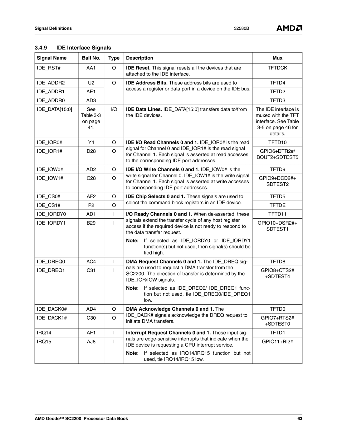
IDE Interface Signals
Serial Ports UARTs Interface Signals
Universal Serial Bus USB Interface Signals
+SDTEST2
GPIO11+IRQ15
DCD2#
GPIO9+IDEIOW1#
Parallel Port Interface Signals
IRRX1 AK8
Fast Infrared IR Port Interface Signals
STB#/WRITE#
FFRAME#
Serial Bus Synchronization. This bit is asserted to syn
14 AC97 Audio Interface Signals
Power Management Interface Signals
General Purpose Wakeup I/Os. These signals each
PWRCNT2 AL7
Suspend Power Plane Control 1 and 2. Control signal
PWRBTN# AH5
PWRCNT1 AK6
Gpio Interface Signals
System Management Interrupt. This is the input to
Debug Monitoring Interface Signals
Jtag Interface Signals
Fast-PCI Bus Monitoring Signals. When enabled, this
Power, Ground and No Connections1
Test and Measurement Interface Signals
3V Analog CRT DAC Power Connections. Low noise power
3V PLL2 Analog Power Connection. Low noise power for PLL2
3V PLL3 Analog Power Connection. Low noise power for PLL3
3V Analog USB Power Connection. Low noise power
32580B
Width Offset Bits
Configuration Block Addresses
General Configuration Block Register Summary
General Configuration Block 32580B
Fpcimon
Ball # Internal Test Signals Name Add’l Dependencies
Other Signal Add’l Dependencies
PMR27
Ball # IDE Signals CRT, Gpio and TFT Signals Name
General Configuration Block
TFT Name Add’l Dependencies
Bit
PP/ACB1/FPCI
Rsvd Reserved. Write to
Ball # Gpio Signals LPC Signals Name Add’l Dependencies
Reserved
32580BGeneral Configuration Block
Bit Description
Offset 3Ch
Interrupt Selection Register Intsel R/W Reset Value 00h
Reset Value xxh
Offset 39h-3Bh
Functional Description
Watchdog Timer
Usage Hints
Watchdog Registers
Watchdog Interrupt
3describes the Watchdog registers
Offset 05h-07h Reserved Rsvd
High-Resolution Timer
High-Resolution Timer Registers
Bit Description Offset 08h-0Bh
Reset Value xxxxxxxxh
Tmclksel Timer Clock Select
Tmen Timer Interrupt Enable
Clock Generators and PLLs
Component Parameters Values Tolerance
1 27 MHz Crystal Oscillator
Crystal Oscillator Circuit Components
Strapped Core Clock Frequency
2 GX1 Module Core Clock
Internal Fast-PCI Clock
Core Clock Frequency
Video Processor Clocks
SuperI/O Clocks
Core Logic Module Clocks
9describes the registers of the clock generator and PLL
Clock Generator Configuration
Clock Registers
66.7 MHz
1514
1110
33.3 MHz
AB1C AB1D AB2C AB2D
Outstanding Features
ISA
Serial Port 3 / Infrared IR Communication Port
PC98 and Acpi Compliant
Parallel Port
Serial Port
Module Architecture
Access
Signals
Internal Internal Signals
LDN Assignments
Configuration Structure/Access
SIO Configuration Options
Index-Data Register Pair
Address Decoding
Default Configuration Setup
Standard Logical Device Configuration Registers
Standard Configuration Registers
SIO Control and Configuration Registers
Logical Device Control and Configuration Registers
Standard Configuration Registers
102
Index F0h-FEh Logical Device Configuration R/W
32580BSuperI/O Module
DMA Channel Select 1 R/W
SID. SIO ID
SIO Control and Configuration Registers
SIO Control and Configuration Register Map
Index Type Name Power Rail Reset Value
Relevant RTC Configuration Registers
Logical Device Control and Configuration
RTC Configuration Registers
Base Address MSB register
Relevant SWC Registers
LDN 01h System Wakeup Control
Relevant IRCP/SP3 Registers
10. IRCP/SP3 Configuration Register
LDN 03h and 08h Serial Ports 1
12. Serial Ports 1 and 2 Configuration Register
Serial Ports 1 and 2 Configuration register
11. Relevant Serial Ports 1 and 2 Registers
13. Relevant ACB1 and ACB2 Registers
14. ACB1 and ACB2 Configuration Register
LDN 05h and 06h ACCESS.bus Ports 1
ACB1 and ACB2 Configuration register
15. Relevant Parallel Port Registers
16. Parallel Port Configuration Register
RTC Clock Generation
X32I External X32O Battery = 0.1 μF
Real-Time Clock RTC
Bus Interface
External Oscillator
Signal Parameters
External Elements
Oscillator Startup
Leap Years
Alarms
Timekeeping Data Format
Daylight Saving
BT1
Power Supply
RTC
18. System Power States
116
Battery-Backed RAMs and Registers
Interrupt Handling
Bit CRC
Index Type Name
RTC Registers
19. RTC Register Map
20. RTC Registers
118
Hours Register HOR R/W Reset Type VPP PUR
Index 05h Hours Alarm Register Hora R/W
CRD is
AMD Geode SC2200 Processor Data Book 119
Index Programmable Month Alarm Register Mona R/W
Index 0Ch RTC Control Register C CRC RO
Index Programmable Century Register CEN R/W
Parameter BCD Format Binary Format
21. Divider Chain Control / Test Selection
22. Periodic Interrupt Rate Encoding
23. BCD and Binary Formats
25. Extended RAM Map
0Eh 7Fh Battery-backed general-purpose Byte RAM
00h 7Fh Battery-backed general-purpose Byte RAM
RTC General-Purpose RAM Map 24. Standard RAM Map
26. Time Range Limits for Ceir Protocols
System Wakeup Control SWC
Event Detection
Offset Type Name Value
SWC Registers
27. Banks 0 and 1 Common Control and Status Register Map
Type Name Value
29. Banks 0 and 1 Common Control and Status Registers
30. Bank 1 Ceir Wakeup Configuration and Control Registers
Ceir Wakeup Range 2 Registers
Bit Description Ceir Wakeup Range 1 Registers
Bank 1, Offset 0Ah IRWTR1L Register R/W
Ceir Pulse Change, Range 1, High Limit
AMD Geode SC2200 Processor Data Book 127
ACCESS.bus Interface
Data Transactions
ABD ABC
ABC ACK
Acknowledge ACK Cycle
ABD MSB
Addressing Transfer Formats
Master Mode
Acknowledge After Every Byte Rule
Arbitration on the Bus
Master Stop
Sending the Address Byte
Master Transmit
Master Receive
Configuration
Slave Mode
32. ACB Registers
ACB Registers
31. ACB Register Map
MASTER. RO
Stop Stop
Inten Interrupt Enable
Saen Slave Address Enable
EN Enable
34. Parallel Port Register Map for Second Level Offset
Legacy Functional Blocks
Parallel Port
33. Parallel Port Register Map for First Level Offset
136
35. Parallel Port Bit Map for First Level Offset
36. Parallel Port Bit Map for Second Level Offset
Type Name
Uart Functionality SP1 and SP2
BSR Bits Bank Selected
38. Bank Selection Encoding
39. Bank 1 Register Map
40. Bank 2 Register Map
SHLCR. Shadow of LCR
41. Bank 3 Register Map
42. Bank 0 Bit Map
MRID. Module and Revision ID
Register Bits Offset
43. Bank 1 Bit Map
44. Bank 2 Bit Map
45. Bank 3 Bit Map
01h Register Throughout Offset 00h All Banks
3.1 IR/SP3 Mode Register Bank Overview
IRCP/SP3 Register and Bit Maps
BSR Bits Bank Selected Functionality
47. Bank Selection Encoding
48. Bank 1 Register Map
49. Bank 2 Register Map
52. Bank 5 Register Map
50. Bank 3 Register Map
51. Bank 4 Register Map
55. Bank 0 Bit Map
53. Bank 6 Register Map
54. Bank 7 Register Map
59. Bank 4 Bit Map
56. Bank 1 Bit Map
57. Bank 2 Bit Map
58. Bank 3 Bit Map
62. Bank 7 Bit Map
60. Bank 5 Bit Map
61. Bank 6 Bit Map
Feature List
Low Pin Count LPC Interface
Config
Integrated Audio
Video Processor Interface
Pserial Interface
Fast-PCI Interface to External PCI Bus
Video Retrace Interrupt
IDE Configuration Registers
PIO Mode
IDE Controller
Physical Region Descriptor Format
DMARDY# Strobe Ideiordy
UltraDMA/33 Signal Definitions
UltraDMA/33 Mode
Stop
Docw
Universal Serial Bus
Sub-ISA Bus Interface
IOCS0#/IOCS1#
AD310 Read AD310 Write
Sub-ISA Support of Delayed PCI Transactions
Sub-ISA Bus Cycles
Fast-PCICLK
Sub-ISA Bus Data Steering
5.4 I/O Recovery Delays
REQ# GNT#
FRAME# IRDY# TRDY# STOP# Bale ISA RD#, IOR#
158
ISA DMA
SD150
AD310
PCI
PCI and Sub-ISA Signal Cycle Multiplexing
Cycle Multiplexed PCI / Sub-ISA Balls
ROM Interface
DMA Channels
FRAME# TRDY#, IRDY#
ROMCS#, DOCCS# IOCS0#, IOCS1# PAR DEVSEL#,STOP#
DMA Controller
DMA Priority
DMA Transfer Modes
DMA Controller Registers
DMA Transfer Types
DMA Address Generation
Programmable Interval Timer
DMA Addressing Capability
DMA Page Registers and Extended Addressing
Mapping
PIC Interrupt Mapping
Programmable Interrupt Controller
Master
PCI Compatible Interrupts
PIC Interrupt Sequence
PIC I/O Registers
PIC Shadow Register
7.2 I/O Port 061h System Control
Fast Keyboard Gate Address 20 and CPU Reset
Keyboard Support
7.1 I/O Port 092h System Control
Power Management Logic
Wakeup Events Capability
Power Management Events
Power Planes Control Signals vs Sleep States
Power Planes vs. Sleep/Global States
AMD Geode SC2200 Processor Data Book 169
Power Button
Power Button Override
Thermal Monitoring
Suspend Modulation
Power Management Programming
CPU Power Management
APM Support
AMD Geode SC2200 Processor Data Book 171
Volt Suspend
Save-to-Disk
Acpi Timer Register
Peripheral Power Management
Device Idle Timers and Traps
General Purpose Timers
F1BAR0+I/O
Power Management SMI Status Reporting Registers
Module
F1BAR0+I/O
Device Power Management Programming Summary
Power Management Programming Summary
Located at F0 Index xxh Unless Otherwise Noted
Integrated Audio
Gpio Interface
Size
11. Physical Region Descriptor Format
Byte
Audio Data Buffer
PRD3
PRD1 PRD2
AMD Geode SC2200 Processor
Audio SMI Related Registers
Trap SMI Enable Register
VSA Technology Support Hardware
VSA Technology
Module Core Logic Module
LPC Interface
IRQ Configuration Registers
Internal IRQ Enable Register
Internal IRQ Control Register
12. Cycle Types
Register Descriptions
PCI Configuration Space and Access Methods
13. PCI Configuration Address Register 0CF8h
Mats are found
Ter’s reset values and page references where the bit for
Register Summary
AMD Geode SC2200 Processor Data Book 185
Width Reset Reference F0 Index Bits
186
32580BCore Logic Module Register Summary
F0BAR1+
15. F0BAR0 Gpio Support Registers Summary
16. F0BAR1 LPC Support Registers Summary
F0BAR0+
F1BAR0+
18. F1BAR0 SMI Status Registers Summary
20h PM2CNT PM2 Control Register 00h 21h-FFh Not Used
19. F1BAR1 Acpi Support Registers Summary
F1BAR1+
00h-03h Pcnt Processor Control Register
190
Width Reset Reference F2 Index Bits
F2BAR4+
Width Reset Reference F3 Index Bits
21. F2BAR4 IDE Controller Support Registers Summary
22. F3 PCI Header Registers for Audio Support Summary
192
Width Reset
23. F3BAR0 Audio Support Registers Summary
F3BAR0+
AMD Geode SC2200 Processor Data Book 193
Width Reset Reference F5 Index Bits
25. F5BAR0 I/O Control Support Registers Summary
F5BAR0+
Width Reference Index Bits
26. Pciusb USB PCI Configuration Register Summary
Name Reset Value
Pciusb
AMD Geode SC2200 Processor Data Book 195
27. Usbbar USB Controller Registers Summary
USBBAR0
196
28. ISA Legacy I/O Register Summary
DMA Page Registers Table
Keyboard Controller Registers Table
Programmable Interval Timer Registers Table
Port Type Name Reference
Programmable Interrupt Controller Registers Table
General Remarks
Chipset Register Space
Bridge, GPIO, and LPC Registers Function
AMD Geode SC2200 Processor Data Book 199
Core Logic Module Bridge, GPIO, and LPC Registers Function
Index 06h-07h PCI Status Register R/W
Data Parity Detected. This bit is set when
Index 0Ch
Index 0Eh PCI Header Type RO Reset Value 80h
Bit Description Index 08h
Index 09h-0Bh
AMD Geode SC2200 Processor Data Book 201
202
Reset Control Register R/W Reset Value 01h
Index 42h
Index 43h
AMD Geode SC2200 Processor Data Book 203
PIT Counter 1 Enable
Reset Value FFFFFFFFh
Reset Value 7Bh
PIT Software Reset
Generate SMI on A20M# Toggle
ROM/AT Logic Control Register R/W Reset Value 98h
206
Index 5Bh Decode Control Register 2 R/W
Index 5Dh
Index 5Ch
INTB# Ball C26 Target Interrupt
INTA# Ball D26 Target Interrupt
208
Reset Value 0000h
Index 72h
Chip Select 1 Positive Decode IOCS1#
Index 77h
Index 74h-75h
Index 76h IOCS0# Control Register R/W
O Chip Select 0 Positive Decode IOCS0#
210
Index 81h Power Management Enable Register 2 R/W
AMD Geode SC2200 Processor Data Book 211
212
Index 82h Power Management Enable Register 3 R/W
Keyboard/Mouse Access Trap
Index 83h Power Management Enable Register 4 R/W
Parallel/Serial Access Trap
Floppy Disk Access Trap
Primary Hard Disk Access Trap
214
Index 84h Second Level PME/SMI Status Mirror Register 1 RO
AMD Geode SC2200 Processor Data Book 215
216
AMD Geode SC2200 Processor Data Book 217
Index 88h General Purpose Timer 1 Count Register R/W
Reserved. Always reads
218
Re-trigger General Purpose Timer 1 on Floppy Disk Activity
Second Millisecond
AMD Geode SC2200 Processor Data Book 219
Index 8Bh General Purpose Timer 2 Control Register R/W
Index 8Dh Video Speedup Timer Count Register R/W
Index 96h
Index 8Fh-92h
Index 93h
Index 94h-95h
AMD Geode SC2200 Processor Data Book 221
Index 9Ah-9Bh Floppy Disk Idle Timer Count Register R/W
Index 97h
Index 98h-99h
Index A8h-A9h Video Overflow Count Register R/W
Index A6h-A7h Video Idle Timer Count Register R/W
Index AAh-ABh Reserved Reset Value 00h 222
Index B4h
Index AEh CPU Suspend Command Register WO
Index AFh Suspend Notebook Command Register WO
Index B0h-B3h
224
Index B9h PIC Shadow Register RO
Index BAh PIT Shadow Register RO
Index C0h-C3h
Index BCh Clock Stop Control Register R/W Reset Value 00h
Reserved. Set to CPU Clock Stop
Index BDh-BFh
Index CFh
Bit Description Mask
Index CDh
Index CEh
AMD Geode SC2200 Processor Data Book 227
Second Level PME/SMI Status Register 1 RC Reset Value 00h
Index F5h Second Level PME/SMI Status Register 2 RC
228
Index F6h Second Level PME/SMI Status Register 3 RC
Reserved . Reads as
AMD Geode SC2200 Processor Data Book 229
Index F7h Second Level PME/SMI Status Register 4 RC
Reserved. Read as
Reserved Reset Value 00h 230
F0 Index 10h, Base Address Register 0 F0BAR0 points to
30. F0BAR0+I/O Offset Gpio Configuration Registers
Gpio Support Registers
232
F0BAR0+I/O Offset 18h is set, this edge generates a PME
316 Reserved. Must be set to
010100 = GPIO20 balls A9, N31 000101
Bank
010010 = GPIO18 ball AG1 000011
010011 = GPIO19 ball C9 000100
234
Reserved. Set to
31. F0BAR1+I/O Offset LPC Interface Configuration Registers
LPC Support Registers
3121
236
AMD Geode SC2200 Processor Data Book 237
Polarity selection
238
Reserved Serial IRQ Enable
Serial IRQ Interface Mode
Number of IRQ Data Frames
AMD Geode SC2200 Processor Data Book 239
LPC Midi Address Select. Selects I/O Port
LPC Game Port 1 Address Select. Selects I/O Port
LPC Game Port 0 Address Select. Selects I/O Port
LPC Floppy Disk Controller Address Select. Selects I/O Port
AMD Geode SC2200 Processor Data Book 241
LPC Error Address 242
Offset 20h-23h Lpcerradd LPC Error Address Register RO
32. F1 PCI Header Registers for SMI Status and Acpi Support
SMI Status and Acpi Registers Function
246
33. F1BAR0+I/O Offset SMI Status Registers
SMI Status Support Registers
AMD Geode SC2200 Processor Data Book 247
Suspend Modulation Enable Mirror. Read to Clear
Offset 02h-03h Top Level PME/SMI Status Register RO/RC
248
AMD Geode SC2200 Processor Data Book 249
Yes To enable SMI generation, set F0 Index 82h6 =
Yes To enable SMI generation, set F0 Index 82h5 =
Bit Description Offset 04h-05h
250
Offset 08h-09h SMI Speedup Disable Register Read to Enable
Offset 0Ah-1Bh
These addresses should not be written Offset 1Ch-1Fh
AMD Geode SC2200 Processor Data Book 251
Bit Description Offset 20h-21h
Offset 22h-23h Second Level Acpi PME/SMI Status Register RC
252
Offset 24h-27h External SMI Register R/W
Second level SMI status is reported at bits 21 RC and 13 RO
Top level SMI status is reported at F1BAR0+00h/02h10
Second level SMI status is reported at bits 23 RC and 15 RO
Second level SMI status is reported at bits 22 RC and 14 RO
254
Offset 28h-4Fh Not Used
Offset 50h-FFh
Clkval Clock Throttling Value. CPU duty cycle
Offset 06h Smicmd OS/BIOS Requests Register R/W
34. F1BAR1+I/O Offset Acpi Support Registers
Acpi Support Registers
256
SCI generation is always enabled
AMD Geode SC2200 Processor Data Book 257
Offset 0Ah-0Bh PM1AEN PM1A PME/SCI Enable Register R/W
1511
Reserved 258
AMD Geode SC2200 Processor Data Book 259
260
Reserved AMD Geode SC2200 Processor Data Book 261
Those selected GPIOs for generation of an SCI
Offset 15h Gpwio Control Register 2 R/W
262
Gpwio Data Register R/W Reset Value 00h
3117
AMD Geode SC2200 Processor Data Book 263
Offset 21h-FFh
Read value for these registers is undefined
314 Bus Mastering IDE Base Address
Reset Value 0502h
Reset Value 010180h
IDE Controller Registers Function
AMD Geode SC2200 Processor Data Book 267
PIOMODE. PIO mode
Core Logic Module IDE Controller Registers Function
268
Reset Value 00009172h
Reset Value 00077771h
Index 48h-4Bh
AMD Geode SC2200 Processor Data Book 269
Bit Description Index 50h-53h
Index 58h-5Bh
Index 60h-FFh
270
IDE Controller Support Registers
Offset 0Ch-0Fh
Offset 09h
Offset 0Ah
Offset 0Bh
Audio Registers Function
37. F3 PCI Header Registers for Audio Configuration
Offset 04h-07h
38. F3BAR0+Memory Offset Audio Configuration Registers
Audio Support Registers
Core Logic Module Audio Registers Function
274
AMD Geode SC2200 Processor Data Book 275
276
Offset 14h-17h Trap SMI and Fast Write Status Register RO/RC
AMD Geode SC2200 Processor Data Book 277
278
Mask Internal IRQ10. Write Only
Mask Internal IRQ15. Write Only
Mask Internal IRQ14. Write Only
Mask Internal IRQ11. Write Only
Reserved. Set to Assert Masked Internal IRQ12
Mask Internal IRQ4. Write Only
Mask Internal IRQ3. Write Only
Assert Masked Internal IRQ14
AMD Geode SC2200 Processor Data Book 281
Bit Description Assert Masked Internal IRQ1
Offset 2Ch-2Fh
Audio Bus Master 1 Command Register R/W Reset Value 00h
Offset 29h Audio Bus Master 1 SMI Status Register RC
Offset 2Ah-2Bh
Offset 34h-37h
Audio Bus Master 2 Command Register R/W Reset Value 00h
Offset 31h Audio Bus Master 2 SMI Status Register RC
Offset 32h-33h
Offset 3Ch-3Fh
Audio Bus Master 3 Command Register R/W Reset Value 00h
Offset 39h Audio Bus Master 3 SMI Status Register RC
Offset 3Ah-3Bh
Offset 44h-47h
Audio Bus Master 4 Command Register R/W Reset Value 00h
Offset 41h Audio Bus Master 4 SMI Status Register RC
Offset 42h-43h
Offset 4Ch-4Fh
Audio Bus Master 5 Command Register R/W Reset Value 00h
Offset 49h Audio Bus Master 5 SMI Status Register RC
Offset 4Ah-4Bh
39. F5 PCI Header Registers for X-Bus Expansion
Bus Expansion Interface Function
Index 28h-2Bh
Bit Description Index 1Ch-1Fh
Index 20h-23h
Index 24h-27h
Index 50h-53h F5BAR4 Mask Address Register R/W
Index 58h F5BARx Initialized Register R/W Reset Value 00h
Index 48h-4Bh F5BAR2 Mask Address Register R/W
Index 4Ch-4Fh F5BAR3 Mask Address Register R/W
40. F5BAR0+I/O Offset X-Bus Expansion Registers
Iostrapidselselect Idsel Strap Override
Three USB transceivers. Default = 128
USB transceivers. Default =
Iotestporten Debug Test Port Enable
292
41. Pciusb USB PCI Configuration Registers
USB Controller Registers Pciusb
Bit Description Index 06h-07h Status Register R/W
Reset Value 08h
Index 0Dh Latency Timer Register R/W
Core Logic Module USB Controller Registers Pciusb
Bit Description Index 10h-13h
Reset Value 0E11h
Reset Value A0F8h
Reset Value 50h
AMD Geode SC2200 Processor Data Book 295
42. USBBAR+Memory Offset USB Controller Registers
Core Logic Module USB Controller Registers Pciusb 32580B
FrameNumberOverflowEnable
HcInterruptEnable Register R/W Reset Value = 00000000h
OwnershipChangeEnable
RootHubStatusChangeEnable
297
Ignore Disable interrupt generation due to Resume Detected
Ignore Disable interrupt generation due to Start of Frame
Offset 28h-2Bh
Offset 38h-3Bh
Reset Value = 00000628h
Reset Value = 01000003h
Bit Description Offset 34h-37h
AMD Geode SC2200 Processor Data Book 299
Read LocalPowerStatusChange. Not supported. Always read
Offset 50h-53h HcRhStatus Register R/W
3018
300 AMD Geode SC2200 Processor Data Book
HcRhPortStatus1 Register R/W Reset Value = 00000000h
Read PortResetStatus
Read PortSuspendStatus
AMD Geode SC2200 Processor Data Book 301
Read PortEnableStatus
Read CurrentConnectStatus
302
319 Reserved. Read/Write 0s
Reset Value = xxh
Offset 60h-9Fh
Offset 100h-103h
304
43. DMA Channel Control Registers
ISA Legacy Register Space
Write
Priority Mode
Timing Mode
32580BCore Logic Module ISA Legacy Register Space
Address Direction
Transfer Mode
Channel Number Mode Select
Bit Description Port 00Bh
308
Write DMA Command Register, Channels
Undefined
Port 0D8h
Bit Description Port 0D2h
Port 0D4h
Port 0D6h
44. DMA Page Registers
45. Programmable Interval Timer Registers
Port 043h R/W
Current Counter Mode BCD Mode
Bit Description Port 042h Write
Counter Value Read
46. Programmable Interrupt Controller Registers
IRQ1 / IRQ9 Mask
Poll Command
Register Read Mode
Bit Description IRQ2 / IRQ10 Mask
IRQ4 / IRQ12 In-Service
Interrupt Service Register IRQ7 / IRQ15 In-Service
IRQ6 / IRQ14 In-Service
IRQ5 / IRQ13 In-Service
47. Keyboard Controller Registers
49. Miscellaneous Registers
48. Real-Time Clock Registers
Bit Description
Graphics-Video Overlay and Blending
General Features
Video Input Port VIP
Hardware Video Acceleration
320
VIP
Mixer/Blender
Video Processor Module
Functional Description
Video Support
VBI Support
Active Video
GenLock
1.1 Direct Video Mode
Video Input Port VIP
Program other VIP bus master support registers
Capture Video Mode
Bob
Program the VIP bus master address registers
AMD Geode SC2200 Processor Data Book 325
Weave
Address not changed during runtime
326
Field Interrupt Capture VBI Mode
Ping-pongs between the two buffers during runtime
AMD Geode SC2200 Processor Data Book 327
Video Block
Video Input Formatter
Line Buffer
Horizontal Downscaler
Horizontal Downscaler with 4-Tap Filtering
Filtering
Ai,j Ai,j+1 Ai+1,jAi+1,j+1
Line Buffers
Formatter
2.5 2-Tap Vertical and Horizontal Upscalers
YUV
Mixer/Blender Block
RGB
RAM
Color/Chroma Key
Valid Mixing/Blending Configurations
YUV to RGB CSC in Video Data Path
Gamma Correction
Cursor Window
Color/Chroma Key and Mixer/Blender
Graphics Window
Video Window
CHROMASEL1
Truth Table for Alpha Blending
Mixing/Blending Operation
Color
334
AMD Geode SC2200 Processor Data Book 335
Vesa DDSC2B and Dpms Support
Integrated DACs
Monitor
T1 is a programmable multiple of frame time T0+T1
Power Sequence
TFT Interface
HSYNC, VSYNC, TFTDE, Tftdck
AMD Geode SC2200 Processor Data Book 337
Divider Phase Charge Loop
Integrated PLL
Compare Pump Filter Divider Out
F4BAR0+
F4BAR0 Video Processor Configuration Registers Summary
Width Reset Reference F4 Index Bits
F4 PCI Header Registers for Video Processor Support Summary
AMD Geode SC2200 Processor Data Book 339
Video Processor Module Register Summary
340
F4BAR2 VIP Support Registers Summary
32580BVideo Processor Module Register Summary
F4BAR2+
Video Processor Module Video Processor Registers Function
Reset Value 0504h
Reset Value 030000h
Video Processor Registers Function
342
Index 3Eh-FFh Reserved
F4 Index 10h, Base Address Register 0 F4BAR0 sets
Base address that allows PCI access to the Video Proces
Video Processor Support Registers F4BAR0
Ddcsdaout DDC Output Data. DDC data bit for output
Offset 04h-07h Display Configuration Register R/W
Tions of the power sequence control lines 1614
3028
AMD Geode SC2200 Processor Data Book 345
Offset 08h-0Bh Video X Position Register R/W
346
Bit Description 100
Block Offset 20h-23h
Reset Value 00001400h
12 PLL2PWREN PLL2 Power-Down Enable
Bit Description Offset 1Ch-1Fh
FLTCO3 Filter Coefficient 3. For the tap-3 filter
DTS Downscale Type Select
Offset 40h-43h Video Downscaler Coefficient Register R/W
FLTCO4 Filter Coefficient 4. For the tap-4 filter
Bit Description Offset 44h-47h CRC Signature Register R/W
Reserved Signen Signature Enable
Reset Value 0000xxxxh
Reset Value 00060000h
350
Top line is in even field. Default Top line is in odd field
Cursor Color Key Register R/W Reset Value 00000000h
100 i.e., shift one line otherwise, leave at
Reserved AMD Geode SC2200 Processor Data Book 351
Incoming graphics stream to be ignored
Offset 60h-63h Alpha Window 1 X Position Register R/W
3125
Reserved 352
3118
Decremented until it is reloaded via bit 17 Loadalpha
Reserved AMD Geode SC2200 Processor Data Book 353
Video Fifo Underflow Empty
Offset 90h-93h
Offset 94h-97h
Offset 400h-403h
Offset 408h-40Bh
Reserved. Set to Genlocktouten GenLock Timeout Enable
Ctgenlocken Enable Continuous GenLock Function
Offset 404h-407h
F4BAR0+Memory Offset Video Processor Configuration Registers
AMD Geode SC2200 Processor Data Book 357
F4BAR2+Memory Offset VIP Configuration Registers
VIP Support Registers F4BAR2
F4 Index 18h, Base Address Register 2 F4BAR2 points to
2322
Capture Store to Memory VBI Data
Capture Store to Memory Video Data
Reserved. Read Only Current Field. Read Only
Start of each field Offset 14h-17h
Bit Description Video Data Capture Active. Read Only
Reserved. Read Only Run Status. Read Only
3110 Reserved
Offset 48h-4Bh VBI Data Pitch Register R/W
Offset 44h-47h VBI Data Even Base Register R/W
Optional Instruction Support
Jtag Mode Instruction Support
Testability Jtag
Mandatory Instruction Support
366
Absolute Maximum Ratings
General Specifications
Power/Ground Connections and Decoupling
Electro Static Discharge ESD
Itor to VSS 233 or 266 MHz 300 MHz
Symbol Parameter Min Typ Max Unit Comments
Operating Conditions
Multipliers 233 or 266 MHz 300 MHz
DC Current
Power Planes of External Interface Signals
Power Plane Signal Names VCC Balls VSS Balls
Power State Parameter Definitions
DC Characteristics for On State
Symbol ParameterNote Min Typ Max Unit Comments
DC Characteristics for Active Idle, Sleep, and Off States
Ball Capacitance and Inductance
Symbol Parameter Min Typ Max Unit Comment
External PU or PD resistor
Pull-Up and Pull-Down Resistors
Balls with PU/PD Resistors
VIO
10. Buffer Types
DC Characteristics
Symbol Description Reference
Wire
Inpci DC Characteristics
Inab DC Characteristics
Inbtn DC Characteristics
INTS1 DC Characteristics
Instrp DC Characteristics
INT DC Characteristics
Ints DC Characteristics
ODn DC Characteristics
Inusb DC Characteristics
Ousb DC Characteristics
Odpci DC Characteristics
N DC Characteristics
Opci DC Characteristics
CLK
AC Characteristics
11. Default Levels for Measurement Switching Parameters
Symbol Parameter Value
Inputs
Memory Controller Interface
Outputs
12.5
12. Memory Controller Timing Parameters
SDCLK30, Sdclkout high time 233 MHz 266 MHz 300 MHz
13.5
MD630 Data Valid Read Data
T1, t2, t3
SDCLK30 Control Output, MA120
BA10, MD630
Vpckin Vref
Video Port 13. Video Input Port Timing Parameters
14. TFT Timing Parameters
CRT and TFT Interface
15. CRT Vesa Compatible DAC RED, GREEN, and Blue Outputs
Symbol Parameter Note Min Max Unit Comments
17. ACCESS.bus Output Timing Parameters
16. ACCESS.bus Input Timing Parameters
AB1C AB2C
AB1C
AB1D AB2D
390
AB1D AB2D AB1C AB2C
AB1D AB2D AB1C
PCI Bus Interface
18. PCI AC Specifications
Equation a Equation B
16VIO
64VIO
Pciclk 0.4 V IO
19. PCI Clock Parameters
20. PCI Timing Parameters
Measurement and Test Conditions
Symbol Value Unit Comments
21. Measurement Condition Parameters
Ms typ
Power
Signals
Input Valid
Bus Width Min
Symbol Parameter Bits Type Comments
Sub-ISA Interface
22. Sub-ISA Timing Parameters
DOCR#/IOR#
Bus Width Min Max Symbol Parameter Bits Type Comments
IOW#/WR# MEMW#/DOCW#
ROMCS#/DOCCS#
IOR#/RD#/TRDE#
MEMR#/DOCR#
D150
DOCCS#/ROMCS#
IOCS10#
IOW#/WR# MEMW#/DOCW# TRDE#
LPC Interface 23. LPC and Serirq Timing Parameters
IDERST# pulse width
IDE signals fall time from 0.9V IO to 0.1V IO = 40 pF
IDE signals rise time from 0.1V IO to 0.9V IO = 40 pF
IDE Interface 24. IDE General Timing Parameters
Width 8-bit min
Mode Symbol Parameter Unit Comments
25. IDE Register Transfer to/from Device Timing Parameters
Cycle time min
IDEIORDY0 2,3
Addr valid1
IDEIOR0# IDEIOW0# Write IDEDATA70
Read IDEDATA70
AMD Geode SC2200 Processor Data Book 405
26. IDE PIO Data Transfer to/from Device Timing Parameters
165 125 100
406
IDEIOR0# IDEIOW0# Write IDEDATA150
Read IDEDATA150
27. IDE Multiword DMA Data Transfer Timing Parameters
408
IDECS10#
IDEDREQ0 IDEDACK0# IDEIOR0# IDEIOW0#
AMD Geode SC2200 Processor Data Book 409
Mode Symbol Parameter Min Max Unit Comments
28. IDE UltraDMA Data Burst Timing Parameters
IDEIRDY0 DSTROBE0
IDEREQ0
STOP0
IDEIOR0# HDMARDY0#
AMD Geode SC2200 Processor Data Book 411
IDEIRDY0 DSTROBE0 at device
IDEDATA150 at device IDEIRDY0 DSTROBE0 at host
IDEDATA150 at host
412
IDEDREQ0 device IDEDACK0# host
IDEIOW0#STOP0 host
IDEIOR0#HDMARDY0#
AMD Geode SC2200 Processor Data Book 413
IDEDREQ0 device
IDEIOW0# STOP0#
IDEADDR20
IDEIOW0# STOP0# host IDEIOR0# HDMARDY0# host
IDEIRDY0 DSTROBE0 device IDEDATA150 device
IDECS01#
IDEIOR0# HSTROBE0# host
DevicetUI IDEDACK0# host
IDEIOW0# STOP0# host
IDEIORDY0 DDMARDY0 device
IDEDATA150 at device
HSTROBE0#
At host
IDEDATA150 At host IDEIOR0# HSTROBE0# at device
AMD Geode SC2200 Processor Data Book 417
IDEDREQ0 device IDEDACK0# host IDEIOW0# STOP0# host
IDEIORDY0# DDMARDY0#
IDEIOR0# HSTROBE0#
418
IDEIORDY0# DDMARDY0# device
IDEDATA150 host IDEADDR20 IDECS01#
IDEDACK0# host
AMD Geode SC2200 Processor Data Book 419
IDEDREQ0 device IDEDACK0 host IDEIOW0# STOP0# host
IDEDATA150 host IDECS01# IDEADDR20
Low Speed Source Note
Full Speed Receiver EOP Width Note
Low Speed Receiver EOP Width Note
Source EOP width
Host upstream
Receiver data jitter tolerance for paired
Consecutive Transitions
Rise Time Fall Time
Differential Data Lines
Differential Data Lines Crossover Points 2.0
Consecutive Transitio ns
Differential Data to SE0 Skew
Data Crossover Level
EOP Width
Setting of the Rxhsc bit bit 5 of the Rccfg register
Modulation signal period
TCPN + Transmitter Sharp-IR and Consumer Remote Control
SIR signal pulse width
FIR
Fast IR Port 31. Fast IR Port Timing Parameters
MIR
STB#
Busy ACK#
Unit Comments
Symbol Parameter Min
33. Enhanced Parallel Port Timing Parameters
Busy
34. ECP Forward Mode Timing Parameters
Extended Capabilities Port ECP
AFD#
BUSY#
35. ECP Reverse Mode Timing Parameters
AC97RST# active low pulse width
Audio Interface AC97 36. AC Reset Timing Parameters
AC97RST# inactive to Bitclk 162.8 Startup delay
Sync inactive to Bitclk startup 162.8 Delay
AC97CLK Vold
38. AC97 Clocks Parameters
SDATAOUT/SYNC SDATAIN, SDATAIN2
39. AC97 I/O Timing Parameters
40. AC97 Signal Rise and Fall Timing Parameters
Bitclk Sdataout
41. AC97 Low Power Mode Timing Parameters
End of Slot 2 to Bitclk Sdatain low
Slot
ONCTL# PWRBTN#
Power Management
Power management event to ONCTL# Assertion
42. PWRBTN# Timing Parameters
PWRBTN# ONTCL# PWRCNT21 POR#
AMD Geode SC2200 Processor Data Book 437
POR# 32KHZ
TDI, TMS hold time
TDI, TMS setup time
Non-test inputs setup time
Jtag Interface 46. Jtag Timing Parameters
AMD Geode SC2200 Processor Data Book 439
Output Signals
Input Signals
TDI TMS TDO
440
Case-to-Ambient Thermal Resistance Example @ 85C
Thermal Characteristics
ΘJC ×C/W
Assume P max = 9W and TA max = 40C Therefore
Heatsink Considerations
Example
Assume P max = 5W and TA max = 40C Therefore
AMD Geode SC2200 Processor Data Book 445
Physical Dimensions
Package Specifications
446
BGU481 Package Bottom View
Degree C Package2
Order Information
Ordering Part Number Core Frequency
MHz
Revision # Revisions / Comments
Data Book Revision History
Table A-1. Revision History