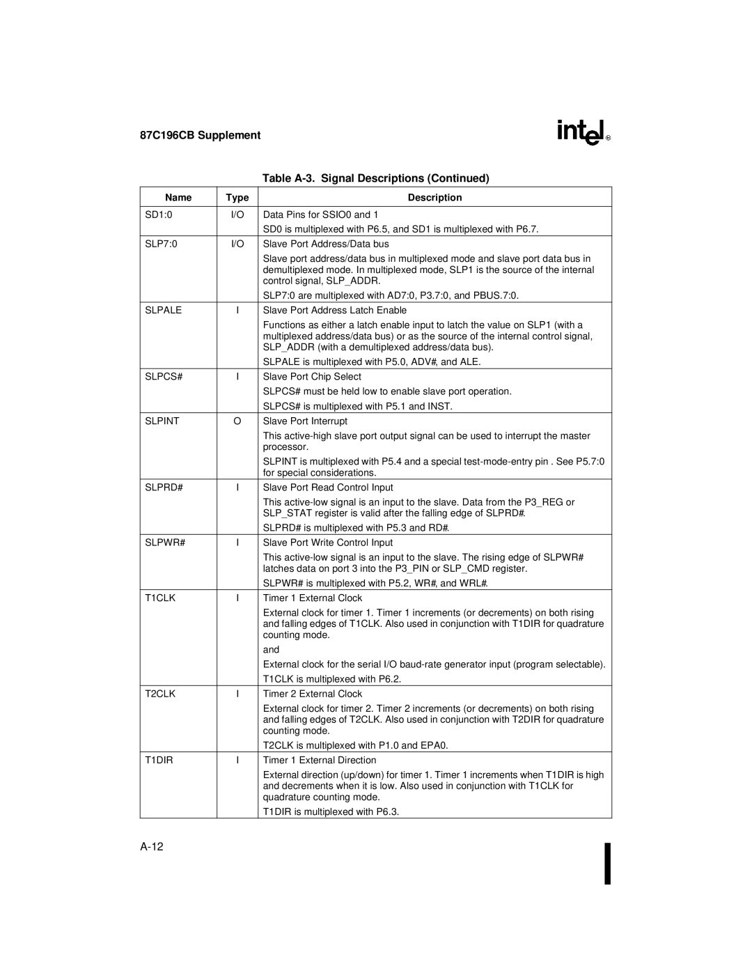
8XC196NT, 87C196CB specifications
The Intel 87C196CB and 8XC196NT are microcontrollers from the C196 family, which was designed to meet the demands of embedded control technology. These microcontrollers are popular in various applications due to their robust architecture, extensive I/O capabilities, and specialized functionality, making them ideal for automotive, industrial, and communication systems.The 87C196CB is distinguished by its 16-bit architecture, offering a balance of processing power and efficiency. It features a 16-bit data bus, which allows for fast data processing, and a 16-bit address bus, supporting up to 64KB of program memory. The microcontroller integrates on-chip memory, including 2KB of ROM and 128 bytes of RAM, which facilitates faster execution of programs and data handling.
One of the standout features of the 87C196CB is its versatility in I/O operations. It comes equipped with 32 general-purpose I/O lines that can be configured for various functions, including input, output, and interrupt handling. This flexibility enables developers to optimize the microcontroller for their specific application needs.
The 8XC196NT builds on the capabilities of its predecessor, offering advanced functionalities such as an enhanced instruction set and integrated peripherals. It includes additional features like timers, serial communication interfaces, and analog-to-digital converters, which expand its usability in complex embedded systems. The 8XC196NT supports multiple addressing modes, allowing for more efficient programming and memory management.
Both microcontrollers utilize innovative technologies that improve performance and power efficiency. The on-chip operating system support aids in real-time processing and multitasking, making them suitable for time-sensitive applications. Power management features are also incorporated, allowing these microcontrollers to operate in low-power modes, which is crucial for battery-operated devices.
The 87C196CB and 8XC196NT microcontrollers are characterized by their reliability and long service life, meeting the stringent demands of industrial applications. Their ability to perform tasks rapidly, combined with their diverse peripheral support, makes them popular choices among engineers and developers designing embedded systems. Overall, the Intel 87C196CB and 8XC196NT microcontrollers remain relevant in the rapidly evolving landscape of embedded technology, facilitating innovative solutions across various industries.

