Users Guide
Submit Documentation Feedback
Contents
MSP-TS430PZ100A MSP-TS430PZ100B
List of Figures
MSP-TS430PZ100B Target Socket Module, PCB
List of Tables
Submit Documentation Feedback
About This Manual
How to Use This Manual
How to Use This Manual
This is an example of a warning statement
Information About Cautions and Warnings
If You Need Assistance FCC Warning
Related Documentation From Texas Instruments
MSP430 development tools documentation
MSP430xxxx device usersguides
Important MSP430 Documents on the CD-ROM and Web
Get Started Now
Kit Contents, eZ430-F2013
Kit Contents, MSP-FET430PIF
Kit Contents, eZ430-T2012
Flash Emulation Tool FET Overview
Kit Contents, eZ430-RF2500T
Kit Contents, eZ430-RF2500
Kit Contents, eZ430-RF2500-SEH
Kit Contents, eZ430-Chronos-xxx
Kit Contents, MSP-FET430xx
Kit Contents, MSP-TS430xx
Kit Contents, FET430Fx137RF900
Individual Kit Contents, MSP-TS430xx
Hardware Installation, MSP-FET430PIF
Kit Contents, EM430Fx137RF900
Hardware Installation, MSP-FET430UIF
Important MSP430 Documents on the CD-ROM and Web
Submit Documentation Feedback
Design Considerations for In-Circuit Programming
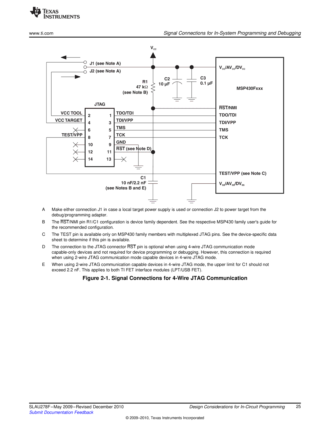
Signal Connections for In-System Programming and Debugging
MSP-FET430PIF, MSP-FET430UIF, MSP-GANG430, MSP-PRGS430
Signal Connections for In-System Programming and Debugging
10 NF/2.2 NF
10 µF 47 KΩ
330 Ω
Signal Connections for 2-Wire Jtag Communication Spy-Bi-Wire
Bootstrap Loader BSL
External Power
Submit Documentation Feedback
Frequently Asked Questions and Known Issues
USB FET
Hardware FAQs
Hardware FAQs
MSP-FET430UIF
Known Issues
Hardware
MSP-TS430PW14
Figure B-1. MSP-TS430PW14 Target Socket Module, Schematic
LED connected to P1.0
Orient Pin 1 MSP430 device Connector J3
Jumper J6 Open to measure current
Table B-1. MSP-TS430PW14 Bill of Materials
MSP-TS430L092
Figure B-3. MSP-TS430L092 Target Socket Module, Schematic
Figure B-4. MSP-TS430L092 Target Socket Module, PCB
Settings of the MSP-TS430L092 Target Socket
Pos Ref Des No No. Per Description DigiKey Part No Comment
Table B-2. MSP-TS430L092 Bill of Materials
MSP-TS430L092 Active Cable
Jumper Description
Table B-3. MSP-TS430L092 JP1 Settings
Pos Ref Des No. Per Description DigiKey Part No Comment
Table B-4. MSP-TS430L092 Active Cable Bill of Materials
MSP-TS430PW24
Figure B-8. MSP-TS430PW24 Target Socket Module, PCB
Table B-5. MSP-TS430PW24 Bill of Materials
MSP-TS430DW28
Figure B-9. MSP-TS430DW28 Target Socket Module, Schematic
Figure B-10. MSP-TS430DW28 Target Socket Module, PCB
Table B-6. MSP-TS430DW28 Bill of Materials
Bootst
Tssop DNP
MSP-TS430PW28
Figure B-11. MSP-TS430PW28 Target Socket Module, Schematic
Figure B-12. MSP-TS430PW28 Target Socket Module, PCB
Pos
Table B-7. MSP-TS430PW28 Bill of Materials1
Description DigiKey Part No Comment
JP9
MSP-TS430PW28A
Figure B-14. MSP-TS430PW28A Target Socket Module, PCB Red
Table B-8. MSP-TS430PW28A Bill of Materials
HRP14H-ND Bootst
MSP-TS430DA38
Figure B-15. MSP-TS430DA38 Target Socket Module, Schematic
Orient pin 1 MSP430 device
Figure B-16. MSP-TS430DA38 Target Socket Module, PCB
Table B-9. MSP-TS430DA38 Bill of Materials
MSP-TS430QFN23x0
Figure B-18. MSP-TS430QFN23x0 Target Socket Module, PCB
MSP430F2370IRHA
Table B-10. MSP-TS430QFN23x0 Bill of Materials
MSP-TS430RSB40
Figure B-19. MSP-TS430RSB40 Target Socket Module, Schematic
Figure B-20. MSP-TS430RSB40 Target Socket Module, PCB
DNP C12
Table B-11. MSP-TS430RSB40 Bill of Materials
DNP C11
Enplassocket
MSP-TS430RHA40A
Figure B-21. MSP-TS430RHA40A Target Socket Module, Schematic
Figure B-22. MSP-TS430RHA40A Target Socket Module, PCB
MSP430N5736IRHA
Table B-12. MSP-TS430RHA40A Bill of Materials
MSP-TS430DL48
Figure B-23. MSP-TS430DL48 Target Socket Module, Schematic
Figure B-24. MSP-TS430DL48 Target Socket Module, PCB
Table B-13. MSP-TS430DL48 Bill of Materials
MSP-TS430RGZ48B
Figure B-25. MSP-TS430RGZ48B Target Socket Module, Schematic
Figure B-26. MSP-TS430RGZ48B Target Socket Module, PCB
MSP430F5342IRGZ
Table B-14. MSP-TS430RGZ48B Bill of Materials
MSP-TS430PM64
Figure B-27. MSP-TS430PM64 Target Socket Module, Schematic
Figure B-28. MSP-TS430PM64 Target Socket Module, PCB
LED connected Connector J5 To pin
DNP C6
Table B-15. MSP-TS430PM64 Bill of Materials
MSP430F417IPM
MSP-TS430PM64A
Figure B-29. MSP-TS430PM64A Target Socket Module, Schematic
Figure B-30. MSP-TS430PM64A Target Socket Module, PCB
Table B-16. MSP-TS430PM64A Bill of Materials
MSP-TS430RGC64B
Figure B-31. MSP-TS430RGC64B Target Socket Module, Schematic
Figure B-32. MSP-TS430RGC64B Target Socket Module, PCB
JP4
Table B-17. MSP-TS430RGC64B Bill of Materials
MSP-TS430RGC64USB
Figure B-34. MSP-TS430RGC64USB Target Socket Module, PCB
P516TR-ND
Table B-18. MSP-TS430RGC64USB Bill of Materials
JP3
DNP Q1
LED JP3QE
IC7
LED1 LEDCHIPLED0603
LED2 LEDCHIPLED0603
MSP-TS430PN80
Figure B-35. MSP-TS430PN80 Target Socket Module, Schematic
Figure B-36. MSP-TS430PN80 Target Socket Module, PCB
MSP430FG439IPN
Table B-19. MSP-TS430PN80 Bill of Materials
MSP-TS430PN80A
Figure B-37. MSP-TS430PN80A Target Socket Module, Schematic
Figure B-38. MSP-TS430PN80A Target Socket Module, PCB
DNP C10
Table B-20. MSP-TS430PN80A Bill of Materials
MSP-TS430PN80USB
Figure B-40. MSP-TS430PN80USB Target Socket Module, PCB
Table B-21. MSP-TS430PN80USB Bill of Materials
IC7
MSP-TS430PZ100
Figure B-41. MSP-TS430PZ100 Target Socket Module, Schematic
Figure B-42. MSP-TS430PZ100 Target Socket Module, PCB
MSP430FG4619IPZ
Table B-22. MSP-TS430PZ100 Bill of Materials
MSP-TS430PZ100A
Figure B-43. MSP-TS430PZ100A Target Socket Module, Schematic
Figure B-44. MSP-TS430PZ100A Target Socket Module, PCB
Table B-23. MSP-TS430PZ100A Bill of Materials
MSP-TS430PZ100B
Figure B-45. MSP-TS430PZ100B Target Socket Module, Schematic
Figure B-46. MSP-TS430PZ100B Target Socket Module, PCB
C12 DNP
Table B-24. MSP-TS430PZ100B Bill of Materials
MSP-TS430PZ5x100
Figure B-48. MSP-TS430PZ5x100 Target Socket Module, PCB
Table B-25. MSP-TS430PZ5x100 Bill of Materials
MSP-TS430PZ100USB
MSP-TS430PZ100USB
Figure B-50. MSP-TS430PZ100USB Target Socket Module, PCB
Table B-26. MSP-TS430PZ100USB Bill of Materials
LED3
LED1, LED2 LEDCHIPLED0603
EM430F5137RF900
Figure B-52. EM430F5137RF900 Target Socket Module, PCB
Reference No. per Description Value Manufacturers Comment
Table B-27. EM430F5137RF900 Bill of Materials
Part Number
RESISTOR/JUMPER, SMT, 0402 ERJ-2GE0R00X Panasonic
Uninstalled CAP Ceramic
RESISTOR, SMT, 0402, Thick
RESISTOR, SMT, Thick FILM, 56K
EM430F6137RF900
Figure B-54. EM430F6137RF900 Target Socket Module, PCB
Pos Ref Des
Table B-28. EM430F6137RF900 Bill of Materials
Description Manufacturer
36a JP3, JP5, JP10 Pin Connector 1x2pin 61300211121
MSP-FET430PIF
Figure B-56. MSP-FET430PIF FET Interface Module, PCB
Figure B-57. MSP-FET430UIF USB Interface, Schematic 1
Figure B-58. MSP-FET430UIF USB Interface, Schematic 2
Figure B-59. MSP-FET430UIF USB Interface, Schematic 3
Figure B-60. MSP-FET430UIF USB Interface, Schematic 4
Figure B-61. MSP-FET430UIF USB Interface, PCB
MSP-FET430UIF Revision History
128
Hardware Installation Guide
Figure C-1. Windows XP Hardware Recognition
Hardware Installation
Figure C-3. Windows XP Driver Location Selection Folder
Figure C-4. Windows XP Driver Installation
133
134
135
Version Changes/Comments
Document Revision History
FCC Warning
Evaluation BOARD/KIT Important Notice
DSP
Products Applications
Rfid