Signal Connections for | www.ti.com |
|
|
| VCC |
|
J1 (SEE NOTE A) |
|
| ||
J2 (SEE NOTE A) |
|
| ||
|
| R1 | C2 | C3 |
|
| 10 µF | 0.1 µF | |
|
| 47 KΩ | ||
|
|
|
| |
|
| (SEE NOTE B) |
|
|
| JTAG |
|
|
|
VCC TOOL | 1 | TDO/TDI |
|
|
2 |
|
|
| |
VCC TARGET | 3 |
|
|
|
4 |
|
|
| |
6 | 5 |
|
|
|
TEST/VPP | 7 | TCK |
|
|
8 |
|
|
| |
10 | 9 | GND |
|
|
| R2 |
| ||
12 | 11 |
|
| |
| 330 Ω |
| ||
|
|
|
| |
14 | 13 |
| (SEE NOTE C) |
|
|
| C1 |
|
|
|
| 2.2 NF |
|
|
|
| (SEE NOTE B) |
|
|
VCC/AVCC/DVCC
MSP430FXXX
RST/NMI/SBWTDIO
TEST/SBWTCK
VSS/AVSS/DVSS
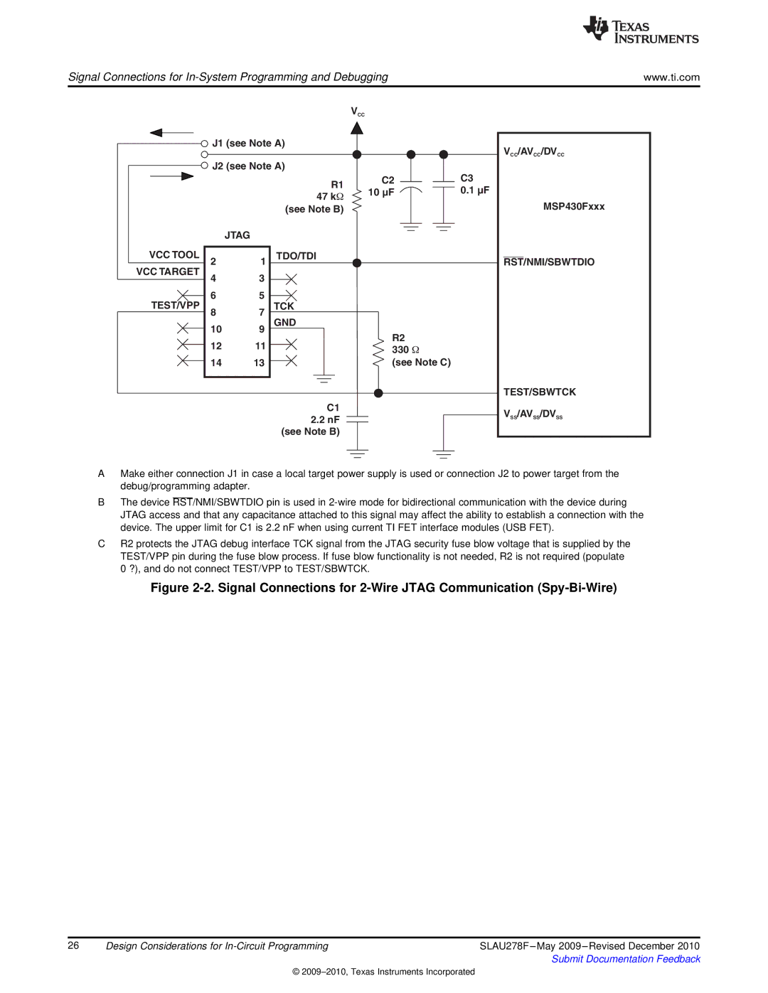
AMake either connection J1 in case a local target power supply is used or connection J2 to power target from the debug/programming adapter.
BThe device RST/NMI/SBWTDIO pin is used in
CR2 protects the JTAG debug interface TCK signal from the JTAG security fuse blow voltage that is supplied by the TEST/VPP pin during the fuse blow process. If fuse blow functionality is not needed, R2 is not required (populate 0 ?), and do not connect TEST/VPP to TEST/SBWTCK.
Figure 2-2. Signal Connections for 2-Wire JTAG Communication (Spy-Bi-Wire)
26 | Design Considerations for | SLAU278F |
|
| Submit Documentation Feedback |
©