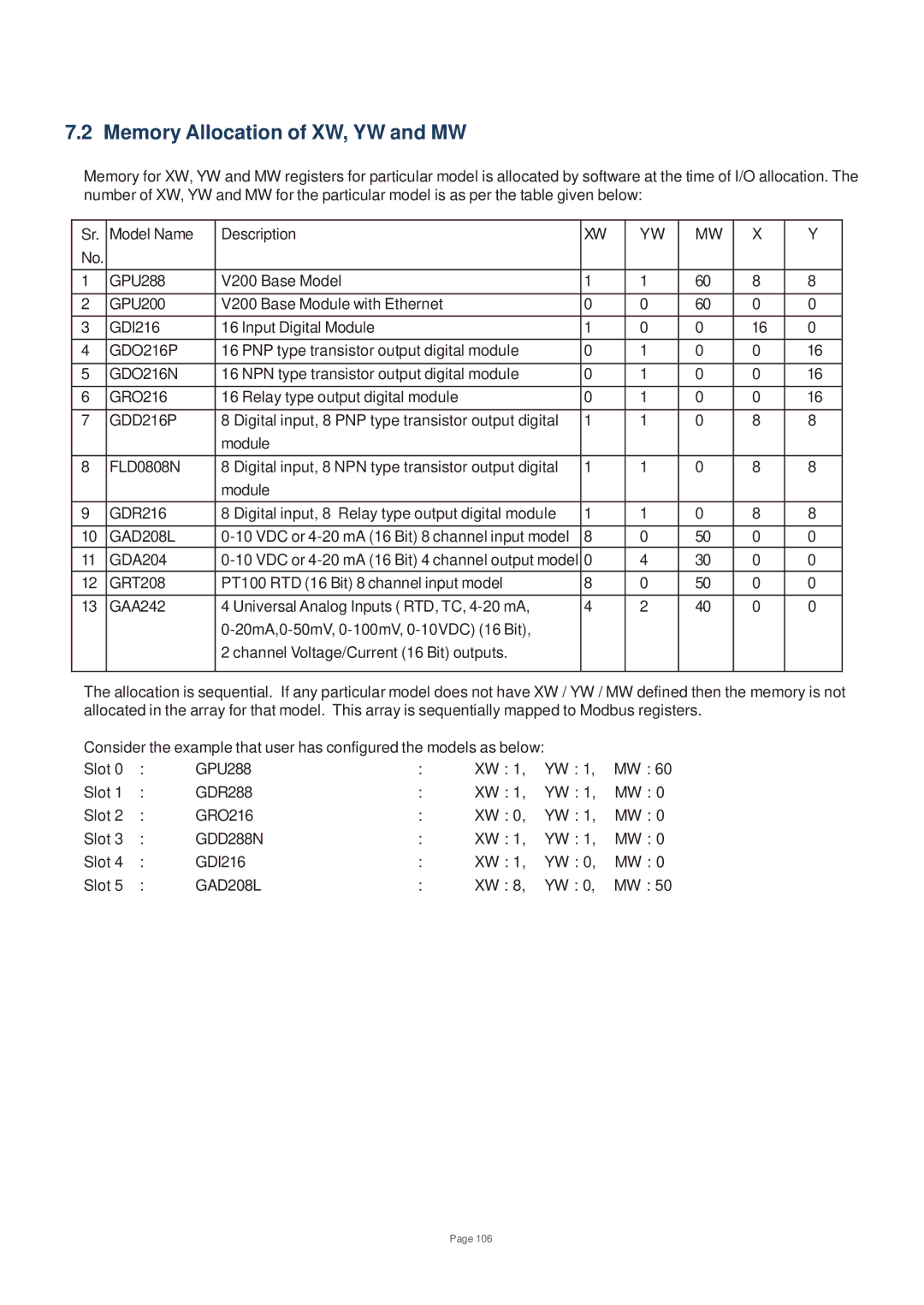
7.2 Memory Allocation of XW, YW and MW
Memory for XW, YW and MW registers for particular model is allocated by software at the time of I/O allocation. The number of XW, YW and MW for the particular model is as per the table given below:
Sr. | Model Name | Description | XW | YW | MW | X | Y |
No. |
|
|
|
|
|
|
|
1 | GPU288 | V200 Base Model | 1 | 1 | 60 | 8 | 8 |
|
|
|
|
|
|
|
|
2 | GPU200 | V200 Base Module with Ethernet | 0 | 0 | 60 | 0 | 0 |
3 | GDI216 | 16 Input Digital Module | 1 | 0 | 0 | 16 | 0 |
4 | GDO216P | 16 PNP type transistor output digital module | 0 | 1 | 0 | 0 | 16 |
|
|
|
|
|
|
|
|
5 | GDO216N | 16 NPN type transistor output digital module | 0 | 1 | 0 | 0 | 16 |
6 | GRO216 | 16 Relay type output digital module | 0 | 1 | 0 | 0 | 16 |
7 | GDD216P | 8 Digital input, 8 PNP type transistor output digital | 1 | 1 | 0 | 8 | 8 |
|
| module |
|
|
|
|
|
8 | FLD0808N | 8 Digital input, 8 NPN type transistor output digital | 1 | 1 | 0 | 8 | 8 |
|
| module |
|
|
|
|
|
9 | GDR216 | 8 Digital input, 8 Relay type output digital module | 1 | 1 | 0 | 8 | 8 |
10 | GAD208L | 8 | 0 | 50 | 0 | 0 | |
11 | GDA204 | 0 | 4 | 30 | 0 | 0 | |
12 | GRT208 | PT100 RTD (16 Bit) 8 channel input model | 8 | 0 | 50 | 0 | 0 |
13 | GAA242 | 4 Universal Analog Inputs ( RTD, TC, | 4 | 2 | 40 | 0 | 0 |
|
|
|
|
|
|
| |
|
| 2 channel Voltage/Current (16 Bit) outputs. |
|
|
|
|
|
|
|
|
|
|
|
|
|
The allocation is sequential. If any particular model does not have XW / YW / MW defined then the memory is not allocated in the array for that model. This array is sequentially mapped to Modbus registers.
Consider the example that user has configured the models as below: |
|
| ||||
Slot 0 | : | GPU288 | : | XW : 1, | YW : 1, | MW : 60 |
Slot 1 | : | GDR288 | : | XW : 1, | YW : 1, | MW : 0 |
Slot 2 | : | GRO216 | : | XW : 0, | YW : 1, | MW : 0 |
Slot 3 | : | GDD288N | : | XW : 1, | YW : 1, | MW : 0 |
Slot 4 | : | GDI216 | : | XW : 1, | YW : 0, | MW : 0 |
Slot 5 | : | GAD208L | : | XW : 8, | YW : 0, | MW : 50 |
Page 106