Detailed Description
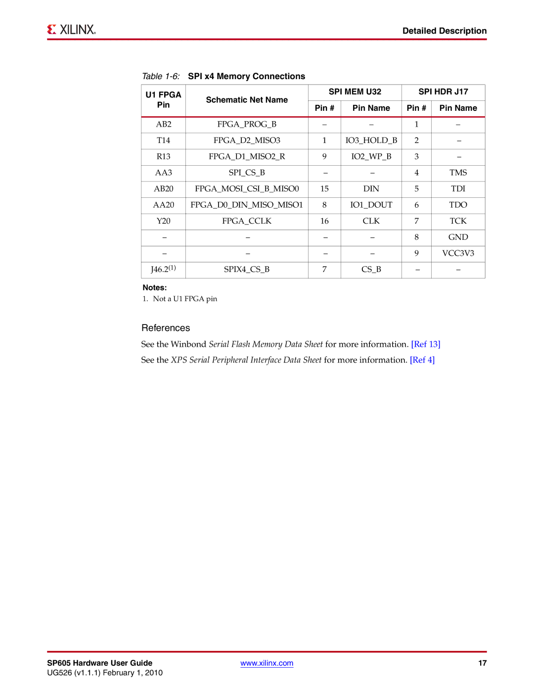
Table 1-6: SPI x4 Memory Connections
U1 FPGA | Schematic Net Name | SPI MEM U32 | SPI HDR J17 | |||
|
|
|
| |||
Pin |
|
|
|
| ||
Pin # | Pin Name | Pin # | Pin Name | |||
| ||||||
|
| |||||
|
|
|
|
|
| |
AB2 | FPGA_PROG_B | – | – | 1 | – | |
|
|
|
|
|
| |
T14 | FPGA_D2_MISO3 | 1 | IO3_HOLD_B | 2 | – | |
|
|
|
|
|
| |
R13 | FPGA_D1_MISO2_R | 9 | IO2_WP_B | 3 | – | |
|
|
|
|
|
| |
AA3 | SPI_CS_B | – | – | 4 | TMS | |
|
|
|
|
|
| |
AB20 | FPGA_MOSI_CSI_B_MISO0 | 15 | DIN | 5 | TDI | |
|
|
|
|
|
| |
AA20 | FPGA_D0_DIN_MISO_MISO1 | 8 | IO1_DOUT | 6 | TDO | |
|
|
|
|
|
| |
Y20 | FPGA_CCLK | 16 | CLK | 7 | TCK | |
|
|
|
|
|
| |
– | – | – | – | 8 | GND | |
|
|
|
|
|
| |
– | – | – | – | 9 | VCC3V3 | |
|
|
|
|
|
| |
J46.2(1) | SPIX4_CS_B | 7 | CS_B | – | – | |
Notes:
1. Not a U1 FPGA pin
References
See the Winbond Serial Flash Memory Data Sheet for more information. [Ref 13]
See the XPS Serial Peripheral Interface Data Sheet for more information. [Ref 4]
SP605 Hardware User Guide | www.xilinx.com | 17 |
UG526 (v1.1.1) February 1, 2010