Xilinx SP605 2. 128 MB DDR3 Component Memory, I/O Voltage Rails, 2 I/O Voltage Rail of FPGA Banks

Models: SP605

1 67
Download 67 pages 13.67 Kb
Page 13
Image 13
I/O Voltage Rails

Detailed Description

I/O Voltage Rails

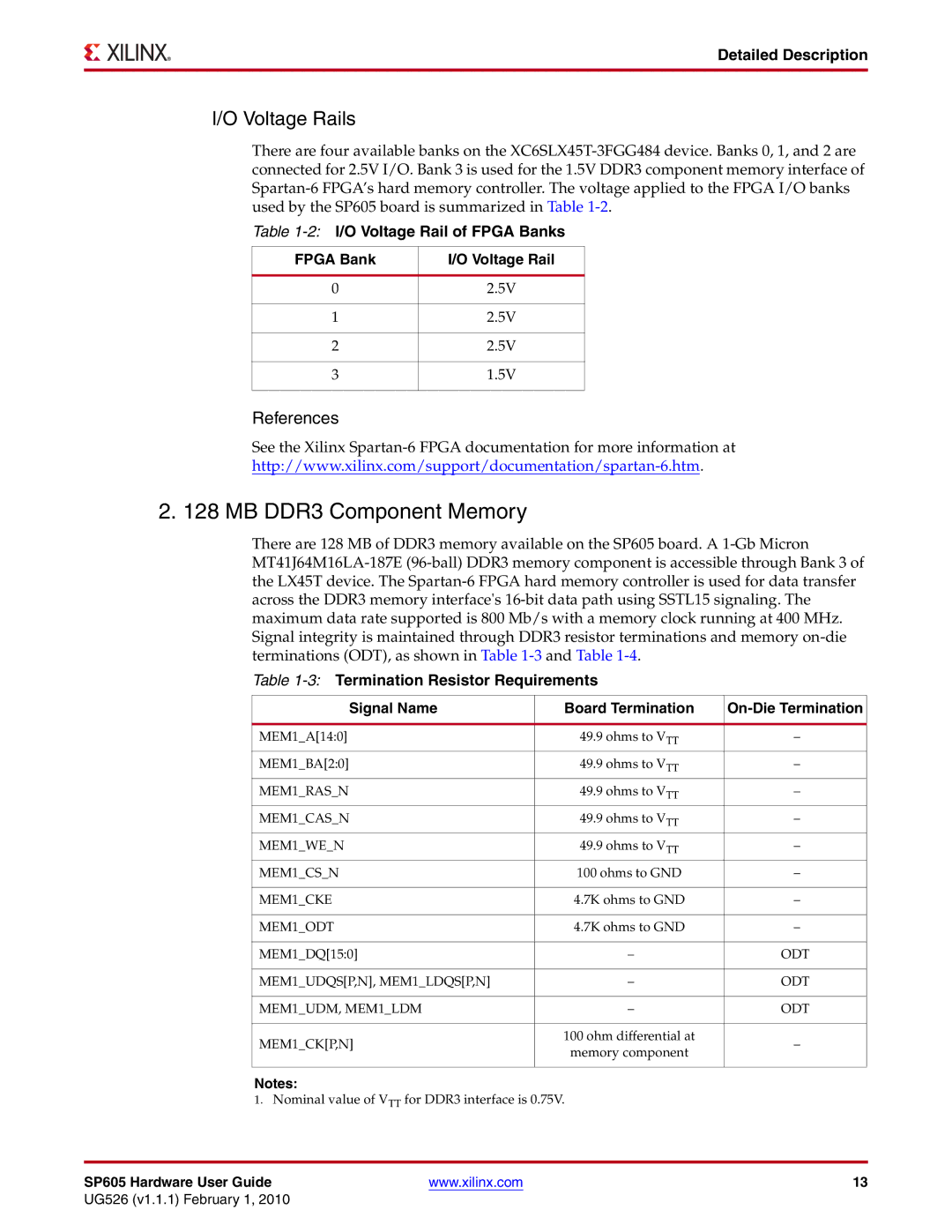
There are four available banks on the XC6SLX45T-3FGG484 device. Banks 0, 1, and 2 are connected for 2.5V I/O. Bank 3 is used for the 1.5V DDR3 component memory interface of Spartan-6 FPGA’s hard memory controller. The voltage applied to the FPGA I/O banks used by the SP605 board is summarized in Table 1-2.

Table 1-2:I/O Voltage Rail of FPGA Banks

FPGA Bank

I/O Voltage Rail


0

2.5V


1

2.5V


2

2.5V


3

1.5V


References

See the Xilinx Spartan-6 FPGA documentation for more information at

http://www.xilinx.com/support/documentation/spartan-6.htm.

2. 128 MB DDR3 Component Memory

There are 128 MB of DDR3 memory available on the SP605 board. A 1-Gb Micron MT41J64M16LA-187E (96-ball) DDR3 memory component is accessible through Bank 3 of the LX45T device. The Spartan-6 FPGA hard memory controller is used for data transfer across the DDR3 memory interface's 16-bit data path using SSTL15 signaling. The maximum data rate supported is 800 Mb/s with a memory clock running at 400 MHz. Signal integrity is maintained through DDR3 resistor terminations and memory on-die terminations (ODT), as shown in Table 1-3and Table 1-4.

Table 1-3:Termination Resistor Requirements

Signal Name

Board Termination

On-Die Termination


MEM1_A[14:0]

49.9 ohms to VTT

MEM1_BA[2:0]

49.9 ohms to VTT


MEM1_RAS_N

49.9 ohms to VTT


MEM1_CAS_N

49.9 ohms to VTT


MEM1_WE_N

49.9 ohms to VTT


MEM1_CS_N

100 ohms to GND


MEM1_CKE

4.7K ohms to GND


MEM1_ODT

4.7K ohms to GND


MEM1_DQ[15:0]

ODT


MEM1_UDQS[P,N], MEM1_LDQS[P,N]

ODT


MEM1_UDM, MEM1_LDM

ODT


MEM1_CK[P,N]

100 ohm differential at

memory component


Notes:

1.Nominal value of VTT for DDR3 interface is 0.75V.

SP605 Hardware User Guide

www.xilinx.com

13

UG526 (v1.1.1) February 1, 2010

Page 13
Image 13
Xilinx SP605 2. 128 MB DDR3 Component Memory, I/O Voltage Rails, 2 I/O Voltage Rail of FPGA Banks, Signal Name, References