Chapter 1: SP605 Evaluation Board
User SIP Header
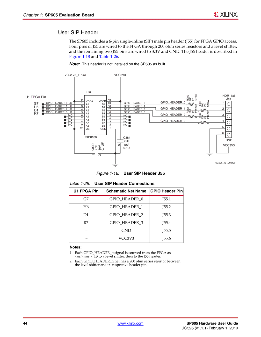
The SP605 includes a
Note: This header is not installed on the SP605 as built.
VCC1V5_FPGAVCC3V3
|
|
|
|
|
|
|
|
|
|
|
| U52 |
|
U1 FPGA Pin |
|
|
|
| 2 |
| VCCA |
| |||||
|
|
|
|
|
| ||||||||
|
|
|
|
|
|
|
|
|
|
| |||
G7 |
|
|
| GPIO_HEADER_0_LS | 1 |
|
| ||||||
|
|
| A1 |
| |||||||||
|
|
|
|
| |||||||||
| GPIO_HEADER_1_LS | 3 |
|
| |||||||||
H6 |
|
|
|
| A2 |
| |||||||
|
|
|
|
| |||||||||
| GPIO_HEADER_2_LS | 4 |
|
| |||||||||
D1 |
|
|
|
|
| A3 |
| ||||||
R7 |
|
|
|
| GPIO_HEADER_3_LS | 5 |
| A4 |
| ||||
|
|
|
|
|
|
| NC | 6 |
| A5 |
| ||
|
|
|
|
|
|
| NC | 7 |
| A6 |
| ||
|
|
|
|
|
|
| NC | 8 |
| A7 |
| ||
|
|
|
|
|
|
| NC | 9 |
| A8 |
| ||
|
|
|
|
|
|
|
|
| 10 |
| OE |
| |
|
|
|
|
|
|
|
|
|
|
|
|
| |
|
|
|
|
|
|
|
|
|
|
|
|
| |
|
|
|
|
|
|
|
|
|
|
| TXB0108 | ||
|
|
|
|
|
|
|
|
|
|
|
| C385 | X5R |
|
|
|
|
|
|
|
|
|
|
|
|
| |
|
|
|
|
|
|
|
|
|
|
| 1 |
| |
|
|
|
|
|
|
|
|
|
|
|
|
|
|
VCCB 1920
B1
B2 18
B3 17
B4 16
B5 15
B6 14
B7 13
B8 12
GND 11
10V | 0.1UF |
|
|
2 |
|
GPIO_HEADER_0 GPIO_HEADER_1 GPIO_HEADER_2 GPIO_HEADER_3
NC
NC
NC
NC
1C384
X5R
210V
0.1UF
GPIO_HEADER_0 | R280 | 200 | 5% | 1/16W | R281 |
| 1/16W | |
1 | 2 | 200 5% | ||||||
GPIO_HEADER_1 | ||||||||
R282 | 200 | 5% | 1/16W | 1 | 2 | |||
GPIO_HEADER_2 | ||||||||
1 | 2 | R283 | 200 5% | 1/16W | ||||
GPIO_HEADER_3 | ||||||||
|
|
|
| 1 |
| 2 | ||
|
|
|
|
|
|
HDR_1x6
J55
1
2
3
4
5
6
DNP
VCC3V3
UG526_18 _092409
Figure 1-18: User SIP Header J55
Table 1-26: User SIP Header Connections
U1 FPGA Pin | Schematic Net Name | GPIO Header Pin |
|
|
|
G7 | GPIO_HEADER_0 | J55.1 |
|
|
|
H6 | GPIO_HEADER_1 | J55.2 |
|
|
|
D1 | GPIO_HEADER_2 | J55.3 |
|
|
|
R7 | GPIO_HEADER_3 | J55.4 |
|
|
|
– | GND | J55.5 |
|
|
|
– | VCC3V3 | J55.6 |
|
|
|
Notes:
1.Each GPIO_HEADER_n signal is sourced from the FPGA as <netname>_LS to a level shifter, then to the J55 header.
2.Each GPIO_HEADER_n net has a 200 ohm series resistor between the level shifter and its respective header pin.
44 | www.xilinx.com | SP605 Hardware User Guide |
|
| UG526 (v1.1.1) February 1, 2010 |