Detailed Description
System ACE CF error and status LEDs indicate the operational state of the System ACE CF controller:
•A blinking red error LED indicates that no CompactFlash card is present
•A solid red error LED indicates an error condition during configuration
•A blinking green status LED indicates a configuration operation is ongoing
•A solid green status LED indicates a successful download
The mode SW1 setting is important because the System ACE CF can fail to configure the FPGA when the mode pins are set to the master modes (Table
With the mode switch SW1 set to 10 (Slave SelectMAP, Table
Every time a CompactFlash card is inserted into the System ACE CF socket, a configuration operation is initiated. Pressing the System ACE CF reset button reprograms the FPGA.
Note: System ACE CF configuration is enabled by way of DIP switch S1. See “17. Switches,” page 46 for more details.
The System ACE CF MPU port (Table
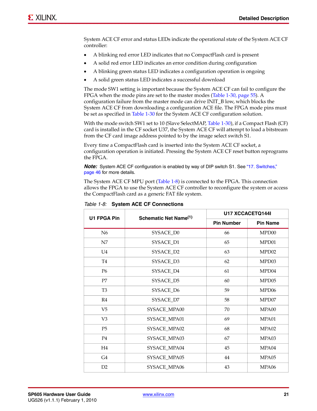
Table 1-8: System ACE CF Connections
| U1 FPGA Pin | Schematic Net Name(1) | U17 XCCACETQ144I | |
|
|
| ||
| Pin Number | Pin Name | ||
|
|
| ||
|
|
|
|
|
| N6 | SYSACE_D0 | 66 | MPD00 |
|
|
|
|
|
| N7 | SYSACE_D1 | 65 | MPD01 |
|
|
|
|
|
| U4 | SYSACE_D2 | 63 | MPD02 |
|
|
|
|
|
| T4 | SYSACE_D3 | 62 | MPD03 |
|
|
|
|
|
| P6 | SYSACE_D4 | 61 | MPD04 |
|
|
|
|
|
| P7 | SYSACE_D5 | 60 | MPD05 |
|
|
|
|
|
| T3 | SYSACE_D6 | 59 | MPD06 |
|
|
|
|
|
| R4 | SYSACE_D7 | 58 | MPD07 |
|
|
|
|
|
| V5 | SYSACE_MPA00 | 70 | MPA00 |
|
|
|
|
|
| V3 | SYSACE_MPA01 | 69 | MPA01 |
|
|
|
|
|
| P5 | SYSACE_MPA02 | 68 | MPA02 |
|
|
|
|
|
| P4 | SYSACE_MPA03 | 67 | MPA03 |
|
|
|
|
|
| H4 | SYSACE_MPA04 | 45 | MPA04 |
|
|
|
|
|
| G4 | SYSACE_MPA05 | 44 | MPA05 |
|
|
|
|
|
| D2 | SYSACE_MPA06 | 43 | MPA06 |
|
|
|
|
|
|
|
|
|
|
SP605 Hardware User Guide | www.xilinx.com |
| 21 | |
UG526 (v1.1.1) February 1, 2010 |
|
|
| |