Device User Guide — 9S12C128DGV1/D V01.05
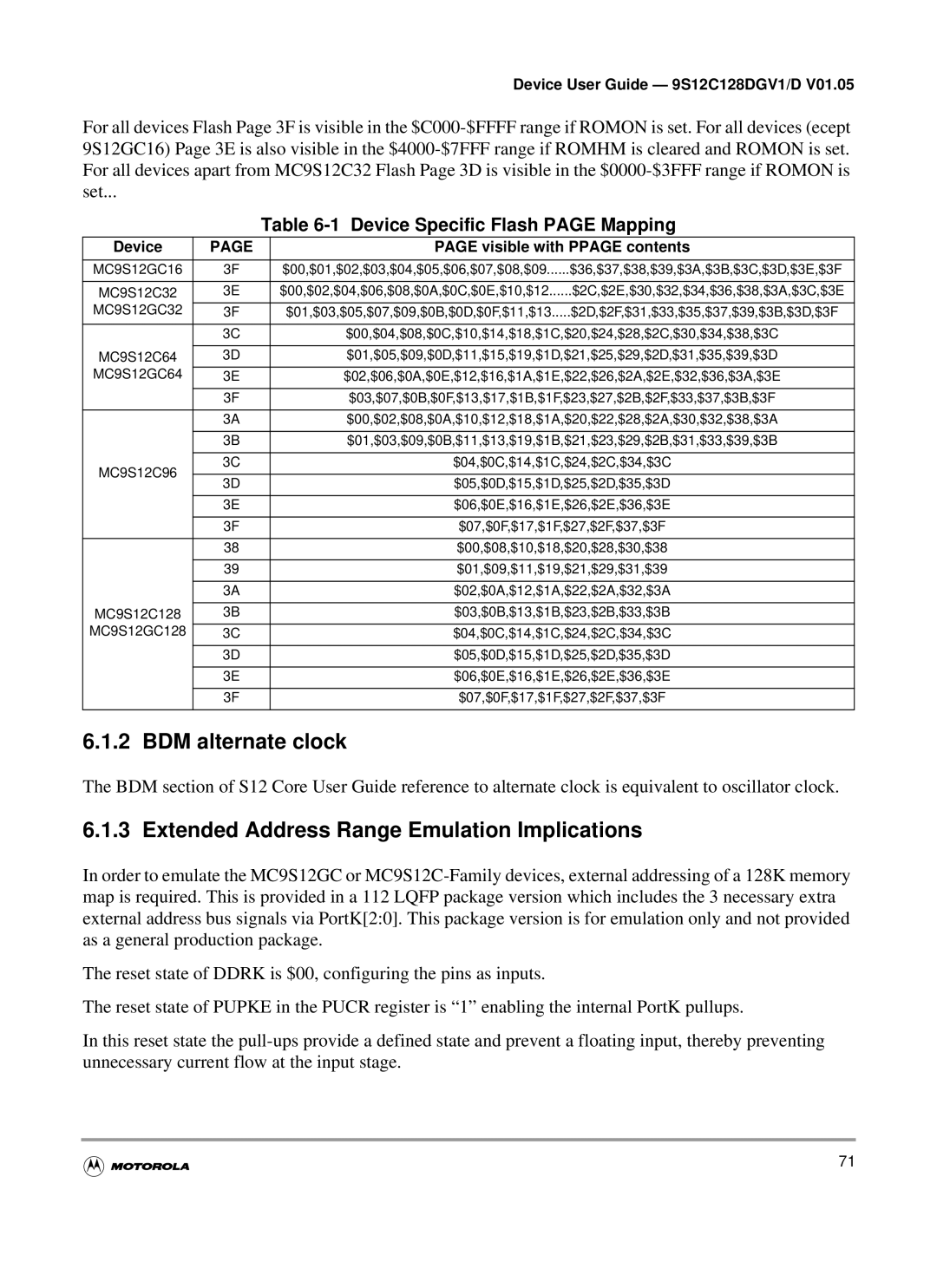
For all devices Flash Page 3F is visible in the
|
| Table | |
Device | PAGE |
| PAGE visible with PPAGE contents |
|
|
|
|
MC9S12GC16 | 3F |
| $00,$01,$02,$03,$04,$05,$06,$07,$08,$09......$36,$37,$38,$39,$3A,$3B,$3C,$3D,$3E,$3F |
|
|
|
|
MC9S12C32 | 3E |
| $00,$02,$04,$06,$08,$0A,$0C,$0E,$10,$12......$2C,$2E,$30,$32,$34,$36,$38,$3A,$3C,$3E |
MC9S12GC32 | 3F |
| $01,$03,$05,$07,$09,$0B,$0D,$0F,$11,$13.....$2D,$2F,$31,$33,$35,$37,$39,$3B,$3D,$3F |
|
|
|
|
| 3C |
| $00,$04,$08,$0C,$10,$14,$18,$1C,$20,$24,$28,$2C,$30,$34,$38,$3C |
|
|
|
|
MC9S12C64 | 3D |
| $01,$05,$09,$0D,$11,$15,$19,$1D,$21,$25,$29,$2D,$31,$35,$39,$3D |
MC9S12GC64 | 3E |
| $02,$06,$0A,$0E,$12,$16,$1A,$1E,$22,$26,$2A,$2E,$32,$36,$3A,$3E |
|
|
|
|
| 3F |
| $03,$07,$0B,$0F,$13,$17,$1B,$1F,$23,$27,$2B,$2F,$33,$37,$3B,$3F |
|
|
|
|
| 3A |
| $00,$02,$08,$0A,$10,$12,$18,$1A,$20,$22,$28,$2A,$30,$32,$38,$3A |
|
|
|
|
| 3B |
| $01,$03,$09,$0B,$11,$13,$19,$1B,$21,$23,$29,$2B,$31,$33,$39,$3B |
|
|
|
|
MC9S12C96 | 3C |
| $04,$0C,$14,$1C,$24,$2C,$34,$3C |
|
|
| |
3D |
| $05,$0D,$15,$1D,$25,$2D,$35,$3D | |
|
| ||
|
|
|
|
| 3E |
| $06,$0E,$16,$1E,$26,$2E,$36,$3E |
|
|
|
|
| 3F |
| $07,$0F,$17,$1F,$27,$2F,$37,$3F |
|
|
|
|
| 38 |
| $00,$08,$10,$18,$20,$28,$30,$38 |
|
|
|
|
| 39 |
| $01,$09,$11,$19,$21,$29,$31,$39 |
|
|
|
|
| 3A |
| $02,$0A,$12,$1A,$22,$2A,$32,$3A |
|
|
|
|
MC9S12C128 | 3B |
| $03,$0B,$13,$1B,$23,$2B,$33,$3B |
MC9S12GC128 | 3C |
| $04,$0C,$14,$1C,$24,$2C,$34,$3C |
|
|
|
|
| 3D |
| $05,$0D,$15,$1D,$25,$2D,$35,$3D |
|
|
|
|
| 3E |
| $06,$0E,$16,$1E,$26,$2E,$36,$3E |
|
|
|
|
| 3F |
| $07,$0F,$17,$1F,$27,$2F,$37,$3F |
|
|
|
|
6.1.2 BDM alternate clock
The BDM section of S12 Core User Guide reference to alternate clock is equivalent to oscillator clock.
6.1.3 Extended Address Range Emulation Implications
In order to emulate the MC9S12GC or
The reset state of DDRK is $00, configuring the pins as inputs.
The reset state of PUPKE in the PUCR register is “1” enabling the internal PortK pullups.
In this reset state the
71