Document Number 9S12C128DGV1/D
Device User Guide 9S12C128DGV1/D
Revision History
Table of Contents
System Clock Description Modes of Operation
Resets and Interrupts
Voltage Regulator Vreg Block Description
HCS12 Core Block Description
Appendix B Electrical Specifications
Appendix E Emulation Information
Appendix C Electrical Specifications
Appendix D Package Information
Device User Guide 9S12C128DGV1/D
List of Figures
Device User Guide 9S12C128DGV1/D
List of Tables
Device User Guide 9S12C128DGV1/D
Device User Guide 9S12C128DGV1/D
Device User Guide 9S12C128DGV1/D
List of MC9S12C and MC9S12GC Family members
Preface
MC9S12C-Family Package Option Summary
Package Device Part Number Mask Temp Flash
TBD 48LQFP
Speed Options 25 = 25MHz bus 16 = 16MHz bus
Part Number Mask Temp Package Speed Description Set
MC9S12C96PCPB16
MC9S12C96PCFA16
MC9S12C96PCFU16
MC9S12C96PVFA16
MC9S12C96PMPB25
MC9S12C96PMFA25
MC9S12C96PMFU25
MC9S12C64PCFA16
MC9S12GC-Family Part Number Coding
MC9S12GC64CPB25 TBD
MC9S12GC64CFA25 TBD
MC9S12GC64CFU25 TBD
MC9S12GC64PVFA25
User Guide Version Document Order Number
Terminology
Document References
Device User Guide 9S12C128DGV1/D
Overview
Features
Introduction
Device User Guide 9S12C128DGV1/D
Modes of Operation
Special Test ModeMotorola use only
MC9S12C-Family Block Diagram
Block Diagram
Address Module Size
Device Memory Map
Device Register Map Overview
MC9S12C128 and MC9S12GC128 User configurable Memory Map
MC9S12C96 User Configurable Memory Map
MC9S12C64 and MC9S12GC64 User Configurable Memory Map
MC9S12C32 and MC9S12GC32 User Configurable Memory Map
Detailed Register Map
MC9S12GC16 User Configurable Memory Map
Ivis
$0010 $0014 MMC map 1 of 4 HCS12 Module Mapping Control
$0017 $0017 MMC map 2 of 4 HCS12 Module Mapping Control
$0015 $0016 INT map 1 of 2 HCS12 Interrupt
$0018 $0018
Miscellaneous Peripherals Device User Guide
$0020 $002F DBG including BKP map 1 of 1 HCS12 Debug
$001F $001F INT map 2 of 2 HCS12 Interrupt
$0030 $0031 MMC map 4 of 4 HCS12 Module Mapping Control
$0034 $003F CRG Clock and Reset Generator
$0040 $006F TIM Timer 16 Bit 8 Channels
$0050
$0070 $007F
Reserved
$00A0 $00C7
$00D0 $00D7
$00C8 $00CF SCI Asynchronous Serial Interface
Reserved $00D8 $00DF SPI Serial Peripheral Interface
TIE
$00E0 $00FF PWM Pulse Width Modulator
$0100 $010F Flash Control Register
Time
$0110 $013F
$0140 $017F Reserved Can Motorola Scalable can MSCAN1
$0140 $017F Can Motorola Scalable can MSCAN1
Reserved $0240 $027F PIM Port Interface Module
$0180 $023F
PRIO7 PRIO6 PRIO5 PRIO4 PRIO3 PRIO2 PRIO1 PRIO0
MODRR4 MODRR3 MODRR2 MODRR1 MODRR0
Ptis
PTIAD7 PTIAD6 PTIAD5 PTIAD4 PTIAD3 PTIAD2 PTIAD1 PTIJ7
PTAD7 PTAD6 PTAD5 PTAD4 PTAD3 PTAD2 PTAD1 PTAD0
DDRAD7
DDRAD2
$0280 $03FF Reserved space
Part ID Assignments
Assigned Part ID Numbers
Memory size registers
MC9S12C32, MC9S12GC32
Device Pinout
Signal Description
PW4/IOC4/PT4
PW0/IOC0/PT0 PW1/IOC1/PT1 PW2/IOC2/PT2 PW3/IOC3/PT3
Pin Assignments in 48 Lqfp for MC9S12C-Family
Signal Properties
Signal Properties Summary
Internal Pull
Resistor Description Function Domain
Device User Guide 9S12C128DGV1/D Internal Pull Pin Name
Pin Initialization for 48 & 52 Pin Lqfp bond-out versions
EXTAL, Xtal Oscillator Pins
Detailed Signal Descriptions
Reset External Reset Pin
Test / VPP Test Pin
6 PA70 / ADDR158 / DATA158 Port a I/O Pins
Bkgd / Taghi / Modc Background Debug, Tag High & Mode Pin
7 PB70 / ADDR70 / DATA70 Port B I/O Pins
8 PE7 / Noacc / Xclks Port E I/O Pin
Pierce Oscillator Connections PE7=0
Colpitts Oscillator Connections PE7=1
10 PE5 / Moda / IPIPE0 Port E I/O Pin
9 PE6 / Modb / IPIPE1 Port E I/O Pin
11 PE4 / ECLK- Port E I/O Pin 4 / E-Clock Output
12 PE3 / Lstrb Port E I/O Pin 3 / Low-Byte Strobe Lstrb
14 PE1 / IRQ Port E input Pin 1 / Maskable Interrupt Pin
16 PAD70 / AN70 Port AD I/O Pins
17 PP7 / KWP7 Port P I/O Pin
18 PP6 / KWP6/ROMCTL Port P I/O Pin
20 PJ76 / KWJ76 Port J I/O Pins
19 PP50 / KWP50 / PW50 Port P I/O Pins
21 PM5 / SCK Port M I/O Pin
22 PM4 / Mosi Port M I/O Pin
Power Supply Pins
5 VRH, VRL ATD Reference Voltage Input Pins
VDDA, Vssa Power Supply Pins for ATD and Vreg
VDDPLL, Vsspll Power Supply Pins for PLL
MC9S12C-Family Power and Ground Connection Summary
Modes of Operation
Chip Configuration Summary
Clock Selection Based on PE7
Mode Selection
Security
Securing the Microcontroller
Low Power Modes
Operation of the Secured Microcontroller
Unsecuring the Microcontroller
Vectors
Resets and Interrupts
Resets
Effects of Reset
Reset Summary Table
HCS12 Core Block Description
Device-specific information
BDM alternate clock
Device Visible with Ppage contents
Extended Address Range Emulation Implications
Device Specific Flash page Mapping
Recommended Printed Circuit Board Layout
Voltage Regulator Vreg Block Description
Vregen
2 VDD1, VDD2, VSS1, VSS2
Component Purpose Type Value
Recommended External Component Values
Recommended PCB Layout 48 Lqfp
Recommended PCB Layout 52 Lqfp
VSS2
Recommended PCB Layout 80 QFP
Recommended PCB Layout for 48 Lqfp Pierce Oscillator
Recommended PCB Layout for 52 Lqfp Pierce Oscillator
Recommended PCB Layout for 80QFP Pierce Oscillator
Clock Reset Generator CRG Block Description
Oscillator OSC Block Description
Timer TIM Block Description
Analog to Digital Converter ATD Block Description
Serial Communications Interface SCI Block Description
RAM Block Description
Flash Block Description
Pulse Width Modulator PWM Block Description
Mscan Block Description
Device User Guide 9S12C128DGV1/D
Power Supply
Appendix a Electrical Characteristics
General
Parameter Classification
Current Injection
Pins
Table A-1 Absolute Maximum Ratings
Num Rating Symbol Min Max Unit
Absolute Maximum Ratings
Model Description Symbol Value Unit
Table A-3 ESD and Latch-Up Protection Characteristics
ESD Protection and Latch-up Immunity
Operating Conditions
Table A-4 Operating Conditions
Power Dissipation and Thermal Characteristics
Rating Symbol Min Typ Max Unit
Pint = IDD ⋅ VDD + Iddpll ⋅ Vddpll + Idda ⋅ Vdda
Num Rating Symbol Min Typ Max Unit
9 I/O Characteristics
Table A-5 Thermal Package Characteristics1
Table A-6 5V I/O Characteristics
Num Rating Symbol Min Typ
Table A-7 3.3V I/O Characteristics
Additional Remarks
Supply Currents
Measurement Conditions
Table A-8 Supply Current Characteristics for MC9S12C32
Stop Current 40 C 27 C
Characteristic Symbol Min Typical Max Unit
Appendix B Electrical Specifications
Voltage Regulator Operating Conditions
Table B-1 Voltage Regulator Electrical Parameters
Output Loads
Chip Power-up and LVI/LVR graphical explanation
Resistive Loads
LVI
Table B-2 Voltage Regulator Capacitive Loads
Num Characteristic Symbol Min Typical Max Unit
Capacitive Loads
Device User Guide 9S12C128DGV1/D
ATD Operating Characteristics In 5V Range
ATD Characteristics
ATD Operating Characteristics In 3.3V Range
Table B-3 ATD Operating Characteristics
Factors influencing accuracy
Table B-4 ATD Operating Characteristics
Source Resistance
Source capacitance
Current injection
Table B-5 ATD Electrical Characteristics
ATD accuracy 3.3V Range
ATD accuracy 5V Range
Table B-6 ATD Conversion Performance
Table B-7 ATD Conversion Performance
1LSB
Figure B-2 ATD Accuracy Definitions
NVM timing
NVM, Flash and Eeprom
Single Word Programming
Row Programming
Mass Erase
Table B-8 NVM Timing Characteristics
Sector Erase
NVM Reliability
Table B-9 NVM Reliability Characteristics
108
Startup
Reset, Oscillator and PLL
Stop Recovery
External Reset
Pseudo Stop and Wait Recovery
Oscillator
XFC Component Selection
Phase Locked Loop
Table B-11 Oscillator Characteristics
XFC Pin
Figure B-3 Basic PLL functional diagram
Jitter Information
⋅ synr +
= max ⎜ ⋅ t nom
Table B-12 PLL Characteristics
116
Num Rating Symbol Min Typ Max
Table B-13 Mscan Wake-up Pulse Characteristics
118
Master Mode
Appendix C Electrical Specifications
Table C-1 Measurement Conditions
Description Value Unit
Num Characteristic Symbol Unit Min Typ Max
Table C-2 SPI Master Mode Timing Characteristics
Mosi Port Data
LSB Master LSB OUT
Input SCK
Slave Mode
Input Miso
Slave MSB
Num Characteristic Symbol Unit Min Typ
Table C-3 SPI Slave Mode Timing Characteristics
Mosi Input Slave MSB OUT
Slave LSB OUT
General Muxed Bus Timing
External Bus Timing
Eclk PE4
PE2 Lstrb PE3 Noacc PE7 PIPO0 PIPO1, PE6,5
Pweh
Table C-4 Expanded Bus Timing Characteristics 5V Range
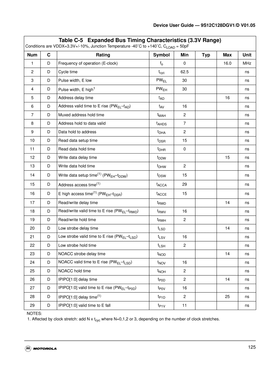
Table C-5 Expanded Bus Timing Characteristics 3.3V Range
126
Appendix D Package Information
80-pin QFP package
Figure D-1 80-pin QFP Mechanical Dimensions case no B
52-pin Lqfp package
Figure D-2 52-pin Lqfp Mechanical Dimensions case no D-03
Section AE-AE Detail AD
48-pin Lqfp package
Appendix E Emulation Information
1 PK20 / XADDR1614
112-pin Lqfp package
134
Device User Guide End Sheet
136