TMS320F2809, TMS320F2808, TMS320F2806
TMS320F2802, TMS320F2801, TMS320C2802
TMS320C2801, TMS320F28016, TMS320F28015
www.ti.com | SPRS230L |
4.6Enhanced Analog-to-Digital Converter (ADC) Module
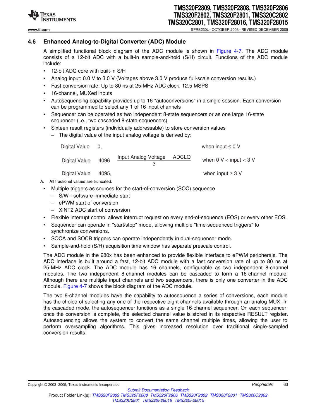
A simplified functional block diagram of the ADC module is shown in Figure
•
•Analog input: 0.0 V to 3.0 V (Voltages above 3.0 V produce
•Fast conversion rate: Up to 80 ns at
•
•Autosequencing capability provides up to 16 "autoconversions" in a single session. Each conversion can be programmed to select any 1 of 16 input channels
•Sequencer can be operated as two independent
•Sixteen result registers (individually addressable) to store conversion values
– The digital value of the input analog voltage is derived by:
Digital Value + 0, |
| when input ≤ 0 V | |
Digital Value + 4096 | Input Analog Voltage * ADCLO | when 0 V < input < 3 V | |
| |||
3 | |||
|
| ||
Digital Value + 4095, |
| when input ≥ 3 V |
A.All fractional values are truncated.
•Multiple triggers as sources for the
–S/W - software immediate start
–ePWM start of conversion
–XINT2 ADC start of conversion
•Flexible interrupt control allows interrupt request on every
•Sequencer can operate in "start/stop" mode, allowing multiple
•SOCA and SOCB triggers can operate independently in
•
The ADC module in the 280x has been enhanced to provide flexible interface to ePWM peripherals. The ADC interface is built around a fast,
The two
Copyright © | Peripherals | 63 |
Submit Documentation Feedback
Product Folder Link(s): TMS320F2809 TMS320F2808 TMS320F2806 TMS320F2802 TMS320F2801 TMS320C2802
TMS320C2801 TMS320F28016 TMS320F28015