Data Manual
ROM
Gpio MUX
ROM Timing C280x only
Typical Operational Power Versus Frequency F2808
Warm Reset
TMS320F2809, TMS320F2808, TMS320F2806
Xclkin Timing Requirements PLL Enabled
Check for
Features
Acquire the appropriate development tools
Getting Started
Download starter software
Download flash programming software
Introduction
Feature TYPE1
Hardware Features 100-MHz Devices
Feature
Hardware Features 60-MHz Devices
TMS320F2809, TMS320F2808 100-Pin PZ Lqfp Top View
Pin Assignments
TMS320F2806 100-Pin PZ Lqfp Top View
On the C280x devices, the VDD3VFL pin is Vddio
TMS320F2801x 100-Pin PZ Lqfp Top View
Bottom View
Signal Descriptions
Signal Descriptions
ADC Signals
Reset
CPU and I/O Power Pins
Gpioa and Peripheral Signals 2
Signal Descriptions
TMS320C2801, TMS320F28016, TMS320F28015
TMS320F2809, TMS320F2808, TMS320F2806
GPIO33
Protected by the CODE-SECURITY Module
Functional Block Diagram
F2809 Memory Map
Memory Maps
F2808 Memory Map
F2806 Memory Map
F2802, C2802 Memory Map
F2801, F28015, F28016, C2801 Memory Map
Addresses of Flash Sectors in F2808
Addresses of Flash Sectors in F2809
Addresses of Flash Sectors in F2806, F2802
Address Range Program and Data Space
Addresses of Flash Sectors in F2801, F28015, F28016
Impact of Using the Code Security Module
Address Flash ROM
Area WAIT-STATES Comments
Wait-states
OTP
H0 Saram
1 C28x CPU
Brief Descriptions
Memory Bus Harvard Bus Architecture
Peripheral Bus
Flash
Real-Time Jtag and Analysis
6 ROM
7 M0, M1 SARAMs
Boot Mode Selection
Boot ROM
8 L0, L1, H0 SARAMs
Disclaimer Code Security Module Disclaimer
Security
Peripheral Interrupt Expansion PIE Block
Low-Power Modes
External Interrupts XINT1, XINT2, Xnmi
Oscillator and PLL
Peripheral Frames 0, 1, 2 PFn
19 32-Bit CPU-Timers 0, 1
General-Purpose Input/Output Gpio Multiplexer
Control Peripherals
Register Map
Serial Port Peripherals
Peripheral Frame 0 Registers1
Access Type
Peripheral Frame 1 Registers1
Name Address Range
Interrupts
Device Emulation Registers
10. Peripheral Frame 2 Registers1
11. Device Emulation Registers
External and PIE Interrupt Sources
MUX
INT1 INT2 INT11 INT12
Intm
External Interrupts
13. PIE Configuration and Control Registers
14. External Interrupt Registers
System Control
OSC and PLL Block
15. PLL, Clocking, Watchdog, and Low-Power Mode Registers1
Crystal
External Clock Signal Toggling 0 −V DD
PLL Mode Remarks Pllstsclkindiv Sysclkout Clkin
17. Possible PLL Configuration Modes
PLL-Based Clock Module
16. Pllcr Register Bit Definitions
Loss of Input Clock
Watchdog Block
18. Low-Power Modes
Low-Power Modes Block
LPMCR010
Oscclk Clkin Sysclkout
Tddrhtddr
32-Bit CPU-Timers 0/1/2
Prdhprd
Pschpsc TCR.4
CPU-Timers 0, 1, 2 Configuration and Control Registers
Enhanced PWM Modules ePWM1/2/3/4/5/6
EPWM1 EPWM2 EPWM3 EPWM4 EPWM5 EPWM6 Size
EPWM Control and Status Registers
#SHADOW
CTR = Zero
Enhanced CAP Modules eCAP1/2/3/4
Hi-Resolution PWM Hrpwm
Ctrovf OVF
Ctrphs
RST
CTR=PRD CTR=CMP
ECAP1 ECAP2 ECAP3 ECAP4
ECAP Control and Status Registers
Size Description
Enhanced QEP Modules eQEP1/2
EQEP1 EQEP2
EQEP Control and Status Registers
Register Description
Address #SHADOW
Enhanced Analog-to-Digital Converter ADC Module
ADCINA0
Sysclkout DSP Adcenclk Halt Hspclk
ADCINA7
ADCINB0 ADCINB7
ADCINB70
ADCINA70
Adclo
Adcrefin
Adcresext
ADC Connections if the ADC Is Not Used
ADC Registers1
ADC Registers
Peripherals
TMS320F2802, TMS320F2801, TMS320C2802
TMS320F2809, TMS320F2808, TMS320F2806
SN65HVD23x
Can Bus
11. eCAN-A Memory Map
12. eCAN-B Memory Map
Register Name
Can Register Map1
ECAN-A ECAN-B
Size Description Address
Serial Communications Interface SCI Modules SCI-A, SCI-B
SCI-B Registers1
SCI-A Registers1
13. Serial Communications Interface SCI Module Block Diagram
When Spibrr = 3 to
11. SPI-B Registers
10. SPI-A Registers
13. SPI-D Registers
12. SPI-C Registers
−−−−−
14. SPI Module Block Diagram Slave Mode
Inter-Integrated Circuit I2C
Gpio MUX Sdaa Scla
14. I2C-A Registers
I2CAENCLK I2C−A C28X CPU Sysclkout
Sysrs
Gpioxnmisel
Gpiolmpsel GPIOXINT1SEL GPIOXINT2SEL
Gpio Control Registers Eallow Protected
15. Gpio Registers
Gpio Data Registers not Eallow Protected
GPAMUX1/2
16. F2808 Gpio MUX Table
GPAMUX1
GPAMUX2
Sync Sysclkout
Time between samples GPyCTRL Reg GPIOx
Software Development Tools
Device and Development Support Tool Nomenclature
Hardware Development Tools
TMS
Temperature Range
Prefix
Device Family
TMS320x280x, 2801x Peripheral Selection Guide
Documentation Support
Literature
Peripheral Guide
Application Programming Interface API Reference
TMS320C28x
TMS320x281x to TMS320x2833x or 2823x Migration Overview
Application Reports and Software
TMS320x280x to TMS320x2833x or 2823x Migration Overview
C28x FPU Primer
Software
SPRA820
Device Support
Absolute Maximum Ratings1
Electrical Specifications
Recommended Operating Conditions
Electrical Characteristics
MIN NOM MAX Unit
Parameter Test Conditions MIN TYP MAX Unit
Sysclkout
Current Consumption
TYP5 MAX6
SCI-A SPI-A ADC
TYP4 MAX5
Peripheral DD Current Module
Reducing Current Consumption
ADC I2C
SCI SPI
Current Consumption Graphs
Total Power
IDD IDDA18
Iddio
Typical Operational Current Versus Frequency C280x
Typical Operational Power Versus Frequency C280x
EMU0 EMU1 Trst TMS TDI TDO TCK DSP GND Tckret Jtagheader
Emulator Connection Without Signal Buffering for the DSP
General Notes on Timing Parameters
Timing Parameter Symbology
Test Load Circuit
85 pF
TMS320x280x Clock Table and Nomenclature 100-MHz Devices
Device Clock Table
XCLKIN1 Timing Requirements PLL Enabled
Clock Requirements and Characteristics
10. XCLKIN1 Timing Requirements PLL Disabled
Input Clock Frequency
Power Management and Supervisory Circuit Solutions
Power Sequencing
12. Power Management and Supervisory Circuit Solutions
Xclkina Xclkoutb
OSCCLK/8A
Xclkout
Xclkout XRS
13. Reset XRS Timing Requirements
OSCCLK/8
General-Purpose Input/Output Gpio
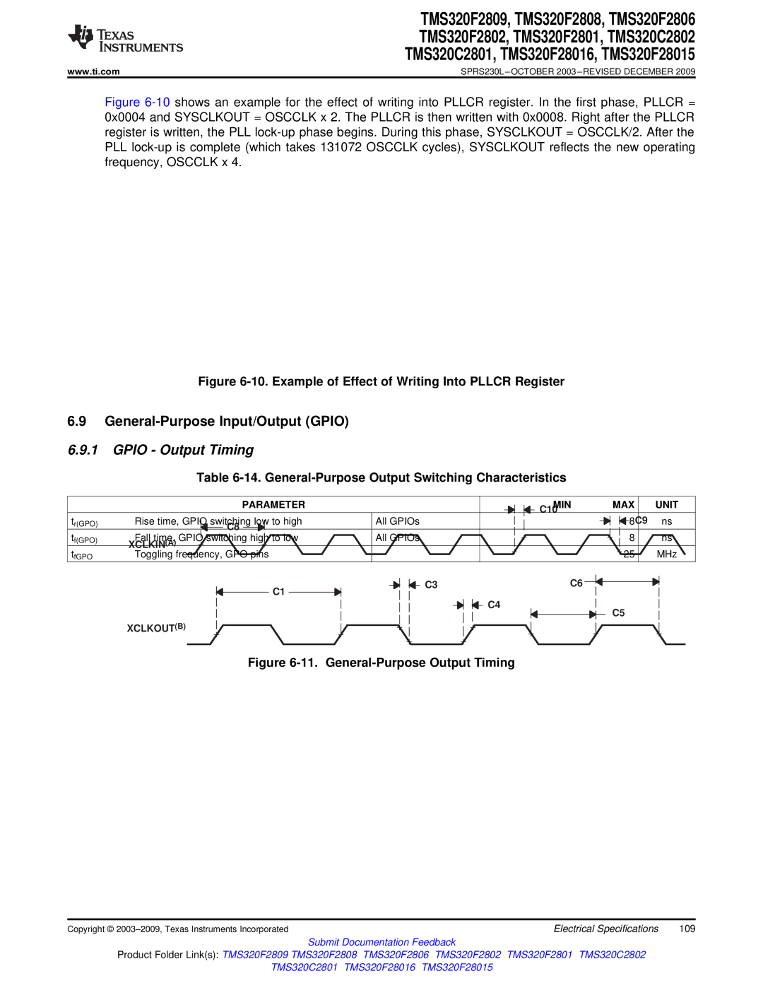
14. General-Purpose Output Switching Characteristics
Gpio Output Timing
Sysclkout Oscclk OSCCLK/2
Gpio Input Timing
Gpio Signal GPxQSELn = 1,0 6 samples
Sysclkout Qualprd = 1 SYSCLKOUT/2
Output From Qualifier
Case
Sampling Window Width for Input Signals
GPIOxn
16. Idle Mode Timing Requirements1
Low-Power Mode Wakeup Timing
17. Idle Mode Switching Characteristics1
Address/Data Internal
19. Standby Mode Switching Characteristics
18. Standby Mode Timing Requirements
Test Conditions MIN NOM MAX Unit
Xclkin Xclkout Standby
21. Halt Mode Switching Characteristics
20. Halt Mode Timing Requirements
Enhanced Control Peripherals
23. ePWM Switching Characteristics
Enhanced Pulse Width Modulator ePWM Timing
Trip-Zone Input Timing
29. eQEP Switching Characteristics
27. eCAP Switching Characteristics
26. Enhanced Capture eCAP Timing Requirement1
MIN TYP MAX Unit
External Interrupt Timing
32. External Interrupt Switching Characteristics1
Parameter
Adcsocbo
Serial Peripheral Interface SPI Master Mode Timing
10.4 I2C Electrical Specification and Timing
33. I2C Timing
Vddio
34. SPI Master Mode External Timing Clock Phase = 0 1 2 3 4
Spisomi Master In Data Must Be Valid
Spisimo
Spistea
35. SPI Master Mode External Timing Clock Phase = 1 1 2 3 4
Clock polarity =
Spiclk
Data Valid
Spisomi
36. SPI Slave Mode External Timing Clock Phase = 01 2 3 4
SPI Slave Mode Timing
Spisimo Data Must Be Valid
37. SPI Slave Mode External Timing Clock Phase = 11 2
On-Chip Analog-to-Digital Converter
ADC Power-Up Control Bit Timing
Converter
Analog Inputs
Conversion Modes
ADCIN0
AT 12.5 MHz Sample n Sample n +
Sequential Sampling Mode Single-Channel Smode =
ADC Clock Remarks
Simultaneous Sampling Mode Dual-Channel Smode =
Detailed Descriptions
44. Flash Endurance for Q Temperature Material1
43. Flash Endurance for a and S Temperature Material1
46. Flash/OTP Access Timing
Flash Timing
ROM Timing C280x only
48. ROM/OTP Access Timing
Sysclkout ns
Flash Flash Random OTP WAIT-STATE
Migration Issues
ADDITIONS, DELETIONS, and Modifications
F280x Thermal Model 100-pin PZ Results
F280x Thermal Model 100-pin GGM Results
C280x Thermal Model 100-pin GGM Results
C280x Thermal Model 100-pin PZ Results
ΨJTC/W
F2809 Thermal Model 100-pin PZ Results
Orderable Device
Package Type Pins Package Qty Eco Plan Lead
Samples
Package Qty Eco Plan Lead
TMS320F2802ZGMS Active
TMS320F2802ZGMA Active
TMS320F2806GGMA Active
Microstar TMS320F2806GGMS Active
TMS320F2809ZGMS Active
TMS320F2809ZGMA Active
10,10 20 TYP
GGM S-PBGA-N100
40 MAX
4145257-3/C 12/01
Page
Plastic Quad Flatpack
PZ S-PQFP-G100
DSP
Products Applications
Rfid