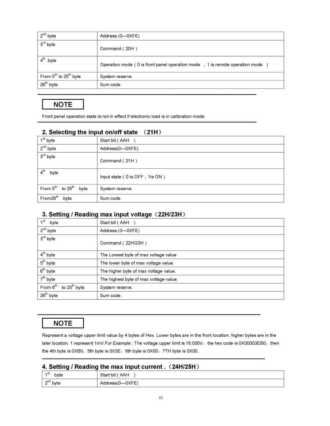
2nd byte | Address |
|
3rd byte | Command(20H) |
|
|
| |
|
|
|
4th .byte | Operation mode(0 is front panel operation mode ,1 is remote operation mode | ) |
| ||
|
|
|
From 5th to 25th byte | System reserve |
|
26th byte | Sum code |
|
NOTE
Front panel operation state is not in effect if electronic load is in calibration mode.
2. Selecting the input on/off state (21H)
1st byte |
| Start bit ( AAH ) |
2nd byte |
| |
3rd byte |
| Command(21H) |
|
| |
|
|
|
4th byte |
| Input state(0 is OFF,1is ON) |
|
| |
|
|
|
From 5th | to 25th byte | System reserve |
|
|
|
From26th | byte | Sum code |
3. Setting / Reading max input voltage(22H/23H)
1st byte | Start bit ( AAH ) |
2nd byte | Address |
3rd byte | Command(22H/23H) |
| |
|
|
4th byte | The Lowest byte of max voltage value |
5th byte | The lower byte of max voltage value. |
6th byte | The higher byte of max voltage value. |
7th byte | The highest byte of max voltage value. |
From 8th to 25th byte | System reserve. |
26th byte | Sum code. |
NOTE
Represent a voltage upper limit value by 4 bytes of Hex. Lower bytes are in the front location, higher bytes are in the later location. 1 represent 1mV.For Example : The voltage upper limit is 16.000V,the hex code is 0X00003EB0,then the 4th byte is 0XB0,5th byte is 0X3E,6th byte is 0X00,7TH byte is 0X00.
4. Setting / Reading the max input current .(24H/25H)
1st byte | Start bit ( AAH ) |
2nd byte |
40