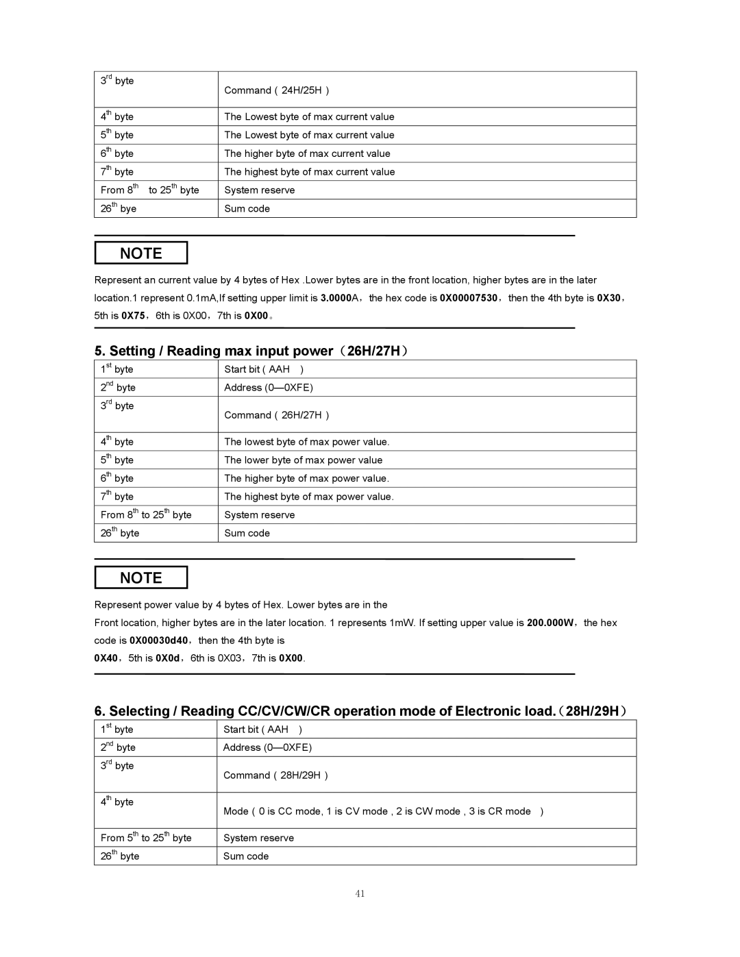
3rd byte | Command(24H/25H) |
| |
|
|
4th byte | The Lowest byte of max current value |
5th byte | The Lowest byte of max current value |
6th byte | The higher byte of max current value |
7th byte | The highest byte of max current value |
From 8th to 25th byte | System reserve |
26th bye | Sum code |
NOTE
Represent an current value by 4 bytes of Hex .Lower bytes are in the front location, higher bytes are in the later location.1 represent 0.1mA,If setting upper limit is 3.0000A,the hex code is 0X00007530,then the 4th byte is 0X30, 5th is 0X75,6th is 0X00,7th is 0X00。
5. Setting / Reading max input power(26H/27H)
1st byte | Start bit ( AAH ) |
2nd byte | Address |
3rd byte | Command(26H/27H) |
| |
|
|
4th byte | The lowest byte of max power value. |
5th byte | The lower byte of max power value |
6th byte | The higher byte of max power value. |
7th byte | The highest byte of max power value. |
From 8th to 25th byte | System reserve |
26th byte | Sum code |
NOTE
Represent power value by 4 bytes of Hex. Lower bytes are in the
Front location, higher bytes are in the later location. 1 represents 1mW. If setting upper value is 200.000W,the hex code is 0X00030d40,then the 4th byte is
0X40,5th is 0X0d,6th is 0X03,7th is 0X00.
6. Selecting / Reading CC/CV/CW/CR operation mode of Electronic load(. 28H/29H)
1st byte | Start bit ( AAH ) |
2nd byte | Address |
3rd byte | Command(28H/29H) |
| |
|
|
4th byte | Mode(0 is CC mode, 1 is CV mode , 2 is CW mode , 3 is CR mode ) |
| |
|
|
From 5th to 25th byte | System reserve |
26th byte | Sum code |
41