Package Information
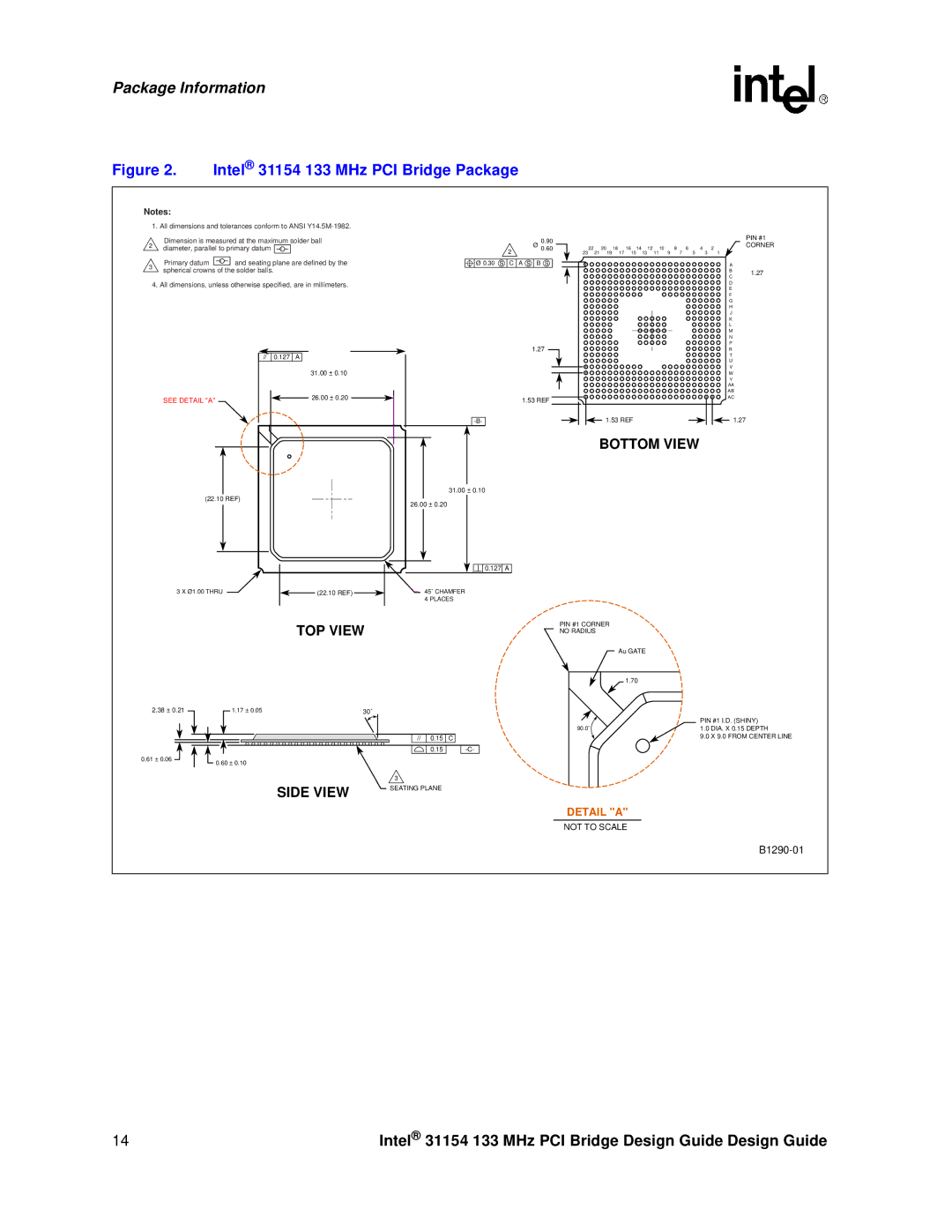
Figure 2. Intel® 31154 133 MHz PCI Bridge Package
Notes:
1. All dimensions and tolerances conform to ANSI
Dimension is measured at the maximum solder ball
2 diameter, parallel to primary datum |
2
0.90 Ø 0.60
|
|
|
|
|
|
|
|
|
|
|
|
| PIN #1 |
| 22 | 20 | 18 | 16 |
| 14 | 12 | 10 | 8 | 6 | 4 | 2 | CORNER |
23 | 21 |
| 19 | 17 | 15 | 13 | 11 | 9 | 7 | 5 | 3 |
| 1 |
3 | Primary datum |
|
| and seating plane are defined by the | |
spherical crowns of the solder balls. | |||||
| |||||
4. All dimensions, unless otherwise specified, are in millimeters. | |||||
|
| // | 0.127 | A |
|
| |
|
| 31.00 ± 0.10 | |||||
SEE DETAIL "A" |
|
|
|
|
| 26.00 ± 0.20 | |
|
|
|
|
| |||
|
|
| |||||
|
|
|
|
|
| ||
|
|
|
|
|
|
|
|
|
|
|
|
|
|
|
|
|
|
|
|
|
|
|
|
(22.10 REF)
3 X Ø1.00 THRU |
|
| (22.10 REF) |
| |||
|
|
|
|
![]()
![]()
![]() Ø 0.30 S C A S B S
Ø 0.30 S C A S B S
1.27
1.53 REF
31.00 ± 0.10
26.00 ± 0.20
0.127 A
45˚ CHAMFER 4 PLACES
A
B 1.27
C
D
E
F
G
H
J
K
L
M
N
P
R
T
U
V
W
Y
AA
AB
AC
1.53 REF |
|
|
|
|
| 1.27 |
|
| |||||
|
|
|
|
|
|
|
BOTTOM VIEW
TOP VIEW
2.38 ± 0.21 | 1.17 ± 0.05 |
| 30˚ |
|
|
|
| // 0.15 | C |
|
|
| 0.15 | |
0.61 ± 0.06 | 0.60 ± 0.10 |
|
|
|
|
|
|
| |
|
|
| 3 |
|
|
| SIDE VIEW | SEATING PLANE |
|
|
|
|
|
PIN #1 CORNER
NO RADIUS
Au GATE
![]() 1.70
1.70
PIN #1 I.D. (SHINY)
90.0˚1.0 DIA. X 0.15 DEPTH
9.0 X 9.0 FROM CENTER LINE
DETAIL "A"
NOT TO SCALE
14 | Intel® 31154 133 MHz PCI Bridge Design Guide Design Guide |