| About This Document |
About This Document | 1 |
|
|
This document provides layout information and guidelines for designing platform or
This document is intended to be used as a guideline only. Intel recommends that you employ best- known design practices with
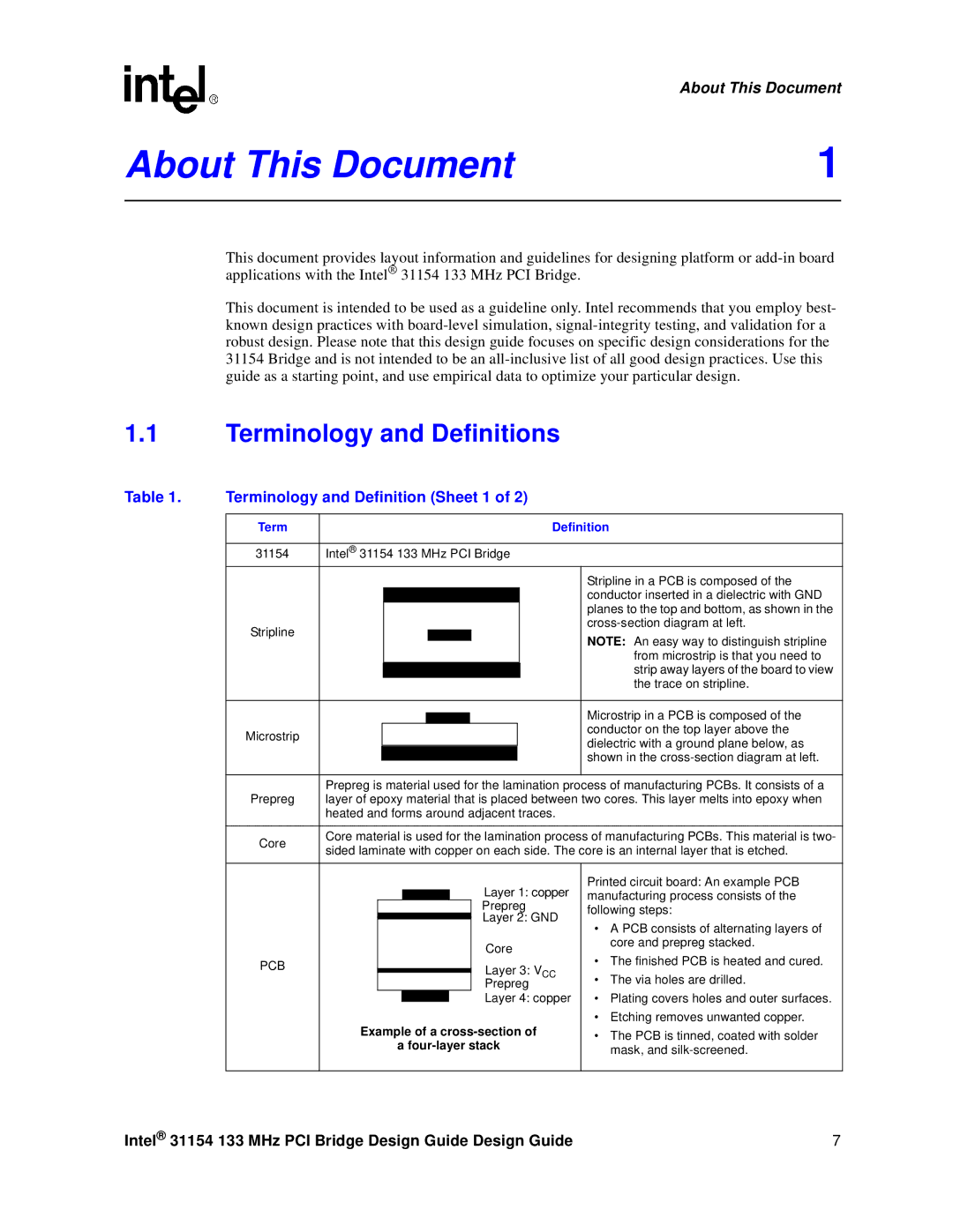
1.1Terminology and Definitions
Table 1. | Terminology and Definition (Sheet 1 of 2) |
| |||||||
|
|
|
|
|
|
|
|
|
|
| Term |
|
|
|
|
|
| Definition | |
|
|
|
|
|
|
|
|
|
|
| 31154 | Intel® 31154 133 MHz PCI Bridge |
| ||||||
|
|
|
|
|
|
|
|
| Stripline in a PCB is composed of the |
|
|
|
|
|
|
|
|
| conductor inserted in a dielectric with GND |
|
|
|
|
|
|
|
|
| planes to the top and bottom, as shown in the |
| Stripline |
|
|
|
|
|
|
| |
|
|
|
|
|
|
|
| NOTE: An easy way to distinguish stripline | |
|
|
|
|
|
|
|
|
| |
|
|
|
|
|
|
|
|
| from microstrip is that you need to |
|
|
|
|
|
|
|
|
| strip away layers of the board to view |
|
|
|
|
|
|
|
|
| the trace on stripline. |
|
|
|
|
|
|
|
|
|
|
|
|
|
|
|
|
|
|
| Microstrip in a PCB is composed of the |
|
|
|
|
|
|
|
|
| |
| Microstrip |
|
|
|
|
|
|
| conductor on the top layer above the |
|
|
|
|
|
|
|
| dielectric with a ground plane below, as | |
|
|
|
|
|
|
|
|
| |
|
|
|
|
|
|
|
|
| shown in the |
|
|
|
|
|
|
|
|
| |
|
|
|
|
|
|
|
|
|
|
|
| Prepreg is material used for the lamination process of manufacturing PCBs. It consists of a | |||||||
| Prepreg | layer of epoxy material that is placed between two cores. This layer melts into epoxy when | |||||||
|
| heated and forms around adjacent traces. |
| ||||||
|
|
|
|
|
|
|
|
| |
| Core | Core material is used for the lamination process of manufacturing PCBs. This material is two- | |||||||
| sided laminate with copper on each side. The core is an internal layer that is etched. | ||||||||
|
| ||||||||
|
|
|
|
|
|
|
|
|
|
|
|
|
|
|
|
| Layer 1: copper | Printed circuit board: An example PCB | |
|
|
|
|
|
|
| manufacturing process consists of the | ||
|
|
|
|
|
|
| Prepreg | following steps: | |
|
|
|
|
|
|
| Layer 2: GND | • A PCB consists of alternating layers of | |
|
|
|
|
|
|
|
|
| |
|
|
|
|
|
|
| Core | core and prepreg stacked. | |
|
|
|
|
|
|
| • The finished PCB is heated and cured. | ||
| PCB |
|
|
|
|
| Layer 3: VCC | ||
|
|
|
|
|
| • The via holes are drilled. | |||
|
|
|
|
|
|
| |||
|
|
|
|
|
|
| Prepreg | ||
|
|
|
|
|
|
|
| ||
|
|
|
|
|
|
| Layer 4: copper | • Plating covers holes and outer surfaces. | |
|
|
|
|
|
|
| |||
|
|
|
|
|
|
|
|
| • Etching removes unwanted copper. |
|
| Example of a | • The PCB is tinned, coated with solder | ||||||
|
|
| a | ||||||
|
|
| mask, and | ||||||
|
|
|
|
|
|
|
|
| |
|
|
|
|
|
|
|
|
|
|
Intel® 31154 133 MHz PCI Bridge Design Guide Design Guide | 7 |