Debug Connectors and Logic Analyzer Connectivity
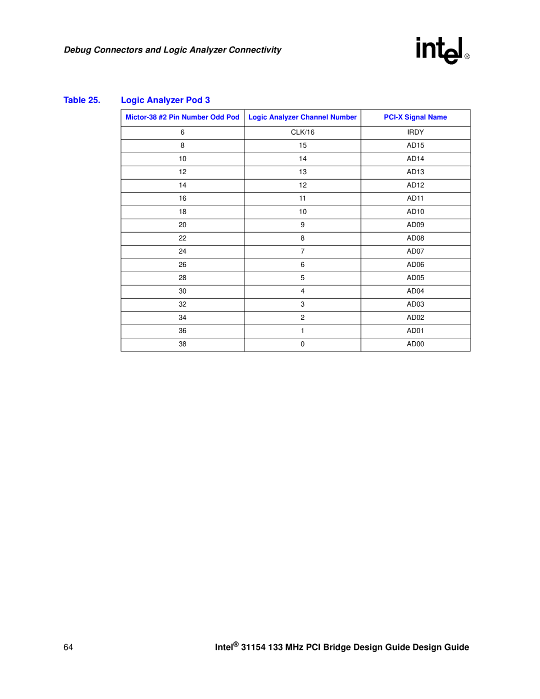
Table 25. | Logic Analyzer Pod 3 |
|
|
|
|
|
|
| Logic Analyzer Channel Number | ||
|
|
|
|
| 6 | CLK/16 | IRDY |
|
|
|
|
| 8 | 15 | AD15 |
|
|
|
|
| 10 | 14 | AD14 |
|
|
|
|
| 12 | 13 | AD13 |
|
|
|
|
| 14 | 12 | AD12 |
|
|
|
|
| 16 | 11 | AD11 |
|
|
|
|
| 18 | 10 | AD10 |
|
|
|
|
| 20 | 9 | AD09 |
|
|
|
|
| 22 | 8 | AD08 |
|
|
|
|
| 24 | 7 | AD07 |
|
|
|
|
| 26 | 6 | AD06 |
|
|
|
|
| 28 | 5 | AD05 |
|
|
|
|
| 30 | 4 | AD04 |
|
|
|
|
| 32 | 3 | AD03 |
|
|
|
|
| 34 | 2 | AD02 |
|
|
|
|
| 36 | 1 | AD01 |
|
|
|
|
| 38 | 0 | AD00 |
|
|
|
|
64 | Intel® 31154 133 MHz PCI Bridge Design Guide Design Guide |