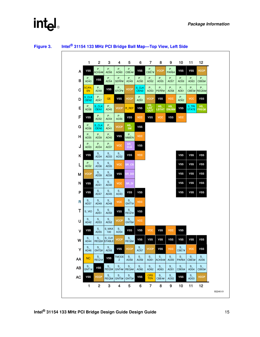
Design Guide
Intel 31154 133 MHz PCI Bridge Design Guide
April
Intel 31154 133 MHz PCI Bridge Design Guide
Contents
Contents
Intel 31154 133 MHz PCI Bridge Design Guide
Figures
Tables
Contents
Intel 31154 133 MHz PCI Bridge Design Guide
Contents
Date
Revision History
Contents
Intel 31154 133 MHz PCI Bridge Design Guide
Terminology and Definition Sheet 1 of
About This Document
1.1 Terminology and Definitions
About This Document
Term
Table 1. Terminology and Definition Sheet 2 of
About This Document
Intel 31154 133 MHz PCI Bridge Design Guide Design Guide
Introduction
PCI-to-PCI Bridge Configurations
Introduction2
2.1 Product Overview
PCI-to-PCI Bridge Architecture Specification, Revision 1.2 compliant
2.2 Features List
Features List
PCI Local Bus Specification, Revision 2.3 compliant
PCI Bus Power Management Interface Specification, Revision
2.3 Related External Specifications
PCI Local Bus Specification, Revision
PCI-to-PCI Bridge Architecture Specification, Revision
THIS PAGE INTENTIONALLY LEFT BLANK
Introduction
Intel 31154 133 MHz PCI Bridge Design Guide Design Guide
Package Information
Package Information
Intel 31154 133 MHz PCI Bridge Design Guide Design Guide
BOTTOM VIEW
Figure 2. Intel 31154 133 MHz PCI Bridge Package
Package Information
Intel 31154 133 MHz PCI Bridge Design Guide Design Guide
AC VSS
Figure 3. Intel 31154 133 MHz PCI Bridge Ball Map-Top View, Left Side
Package Information
Intel 31154 133 MHz PCI Bridge Design Guide Design Guide
VCCA
Package Information
Intel 31154 133 MHz PCI Bridge Design Guide Design Guide
13 14 15 16 17 18 19 20
Package Information
3.1 Total Signal Count
Total Signal Count
Signals
Package Information
THIS PAGE INTENTIONALLY LEFT BLANK
Intel 31154 133 MHz PCI Bridge Design Guide Design Guide
Terminations4
Terminations
Pull-Up/Pull-Down Terminations Sheet 1 of
Terminations
Pull-Up/Pull-Down Terminations Sheet 2 of
Signal
Secondary PCI Signals
Intel 31154 133 MHz PCI Bridge Design Guide Design Guide
Pull-Up/Pull-Down Terminations Sheet 3 of
Signal
Terminations
Intel 31154 133 MHz PCI Bridge Design Guide Design Guide
Pull-Up/Pull-Down Terminations Sheet 4 of
Signal
Terminations
Terminations
Pull-Up/Pull-Down Terminations Sheet 5 of
Signal
resistor default
Intel 31154 133 MHz PCI Bridge Design Guide Design Guide
Pull-Up/Pull-Down Terminations Sheet 6 of
Signal
Terminations
“Power Sequencing” on page
Pull-Up/Pull-Down Terminations Sheet 7 of
Signal
“Power Sequencing” on page
Intel 31154 133 MHz PCI Bridge Design Guide Design Guide
Pull-Up/Pull-Down Terminations Sheet 8 of
Signal
Terminations
Intel 31154 133 MHz PCI Bridge Design Guide Design Guide
Pull-Up/Pull-Down Terminations Sheet 9 of
Signal
Terminations
Terminations
THIS PAGE INTENTIONALLY LEFT BLANK
Intel 31154 133 MHz PCI Bridge Design Guide Design Guide
PCI/PCI-X Interface
PCI/PCI-X Interface
5.1 PCI/PCI-X Voltage Levels
5.2 Interrupt Routing
IDSEL Mapping
5.3 IDSEL Lines
5.3.1 Primary IDSEL Line
5.3.2 Secondary IDSEL Lines
5.3.4 Secondary Clock Control
5.5 Opaque Memory Region Enable
5.3.3 Secondary IDSEL Masking
5.4 CompactPCI* Hot Swap Mode Select
PCI/PCI-X Interface
5.6 PCI-X Initialization Clocking Modes
5.6.1 Primary PCI Clocking Mode
5.6.2 Secondary PCI Clocking Mode
Intel 31154 133 MHz PCI Bridge Design Guide Design Guide
PCI-X Clocking Modes
Secondary Bus Frequency Initialization
PCI/PCI-X Interface
Intel 31154 133 MHz PCI Bridge Design Guide Design Guide
5.6.3 Primary-to-Secondary Frequency Limits
PCI-X Initialization Pattern
PCI/PCI-X Interface
Routing Guidelines
Routing Guidelines
Intel 31154 133 MHz PCI Bridge Design Guide Design Guide
6.1 Crosstalk
Figure 6. Crosstalk Effects on Trace Distance and Height
Routing Guidelines
Intel 31154 133 MHz PCI Bridge Design Guide Design Guide
Figure 7. PCB Ground Layout Around Connectors
6.2 EMI Considerations
Routing Guidelines
Routing Guidelines
6.3 Power Distribution and Decoupling
6.3.1 Decoupling Recommendations
Table 11. Intel 31154 133 MHz PCI Bridge Decoupling Recommendations
6.4 Trace Impedance
Routing Guidelines
Intel 31154 133 MHz PCI Bridge Design Guide Design Guide
Routing Guidelines
THIS PAGE INTENTIONALLY LEFT BLANK
Intel 31154 133 MHz PCI Bridge Design Guide Design Guide
PCI-X Layout Guidelines
Add-in Card Routing Parameters
7.1 PCI Clock Layout Guidelines
PCI-X Layout Guidelines
Intel 31154 133 MHz PCI Bridge Design Guide Design Guide
Notes -3%%%
####
Intel
####%,%!#%#
Intel 31154 133 MHz PCI Bridge Design Guide Design Guide
7.2 PCI-X Topology Layout Guidelines
PCI-X Slot Guidelines
PCI-X Layout Guidelines
Wiring Lengths for 133 MHz Slot
7.2.1 Single Slot at 133 MHz
Figure 9. Single-Slot Point-to-Point Topology
B3058-01
Wiring Lengths for Embedded 133 MHz Design
PCI-X Layout Guidelines
Intel 31154 133 MHz PCI Bridge Design Guide Design Guide
PCI-X Layout Guidelines
Figure 11. Dual-Slot Configuration
Wiring Lengths for 100 MHz Dual-Slot
7.2.2 Dual-Slot at 100 MHz
Lower AD Bus
Wiring Lengths for Embedded 100 MHz Design
PCI-X Layout Guidelines
Intel 31154 133 MHz PCI Bridge Design Guide Design Guide
PCI-X Layout Guidelines
Table 18. Wiring Lengths for 66 MHz Quad-Slot Sheet 1 of
7.2.3 Quad-Slots at 66 MHz
Figure 13. Quad-Slots 66 MHz Topology
Lower AD Bus
Table 18. Wiring Lengths for 66 MHz Quad-Slot Sheet 2 of
PCI-X Layout Guidelines
Intel 31154 133 MHz PCI Bridge Design Guide Design Guide
PCI-X Layout Guidelines
Figure 14. Embedded Intel 31154 133 MHz PCI Bridge Wiring for 66 MHz
Wiring Lengths for Embedded 66 MHz Design
7.2.3.1 Embedded Intel 31154 133 MHz PCI Bridge Application at 66 MHz
PCI-X Layout Guidelines
7.2.4.1 Embedded PCI-X Specification PICMG 1.2 Overview
7.2.4 PCI-X at 33 MHz
7.2.4.2 PICMG 1.2 System Overview
Figure 15. An Example of an ePCI-X System
PCI-X Layout Guidelines
Intel 31154 133 MHz PCI Bridge Design Guide Design Guide
Table 20. Wiring Lengths for PICMG 1.2 Backplane
Figure 16. PCI-X Data Bus PICMG 1.2 Style Backplane
PCI-X Layout Guidelines
SlotN
Table 21. PCI-X Clock Wiring Lengths for PICMG Backplane
Figure 17. PCI-X Clock PICMG 1.2 Style Backplane
Slot1
PCI-X Layout Guidelines
THIS PAGE INTENTIONALLY LEFT BLANK
Intel 31154 133 MHz PCI Bridge Design Guide Design Guide
Power Considerations
8.1 Analog Power Pins
Power Considerations
Intel 31154 133 MHz PCI Bridge Design Guide Design Guide
8.2 Power Sequencing
Intel 133 MHz PCI Bridge
Power Considerations
133 MHz PCI Bridge
Figure 21. Intel IQ31154 Customer Reference Board Block Diagram
Customer Reference Board
Intel
Customer Reference Board Stackup
Customer Reference Board
Intel 31154 133 MHz PCI Bridge Design Guide Design Guide
Debug Connectors and Logic Analyzer Connectivity10
10.1 Probing PCI-X Signals
Debug Connectors and Logic Analyzer Connectivity
Logic Analyzer Pod
Debug Connectors and Logic Analyzer Connectivity
Intel 31154 133 MHz PCI Bridge Design Guide Design Guide
Debug Connectors and Logic Analyzer Connectivity
Logic Analyzer Pod
Intel 31154 133 MHz PCI Bridge Design Guide Design Guide
AD15
Debug Connectors and Logic Analyzer Connectivity
Logic Analyzer Pod
Intel 31154 133 MHz PCI Bridge Design Guide Design Guide
Debug Connectors and Logic Analyzer Connectivity
Logic Analyzer Pod
Intel 31154 133 MHz PCI Bridge Design Guide Design Guide
Debug Connectors and Logic Analyzer Connectivity
PCI-X Signal Name
Logic Analyzer Pod
Intel 31154 133 MHz PCI Bridge Design Guide Design Guide
Debug Connectors and Logic Analyzer Connectivity
The recommended placement of the Mictor connectors is at either end of the bus segment. The Mictors are placed at the end of a stub that must be as short as possible, and are then daisy-chained off either end of the bus. When there is not enough room to place the Mictors at least 0.5 from the target, an alternate method can be used. This alternate method is to place the logic analyzer termination circuitry on the target and then extend the etch from the end of the termination circuitry over to the Mictor connectors. The connection from the Mictors to the logic analyzer must then be made with the E5351A. The E5346A contains the logic analyzer termination circuitry, and the E5351A does not
Logic Analyzer Pod
Debug Connectors and Logic Analyzer Connectivity
THIS PAGE INTENTIONALLY LEFT BLANK
Intel 31154 133 MHz PCI Bridge Design Guide Design Guide
Maximum Power
Thermal Solutions
Thermal Solutions
Table 29. Operational Power
Thermal Solutions
THIS PAGE INTENTIONALLY LEFT BLANK
Intel 31154 133 MHz PCI Bridge Design Guide Design Guide
Table 30. Design Reference Material
References12
12.1 Related Documents
References
References
THIS PAGE INTENTIONALLY LEFT BLANK
Intel 31154 133 MHz PCI Bridge Design Guide Design Guide