Routing Guidelines
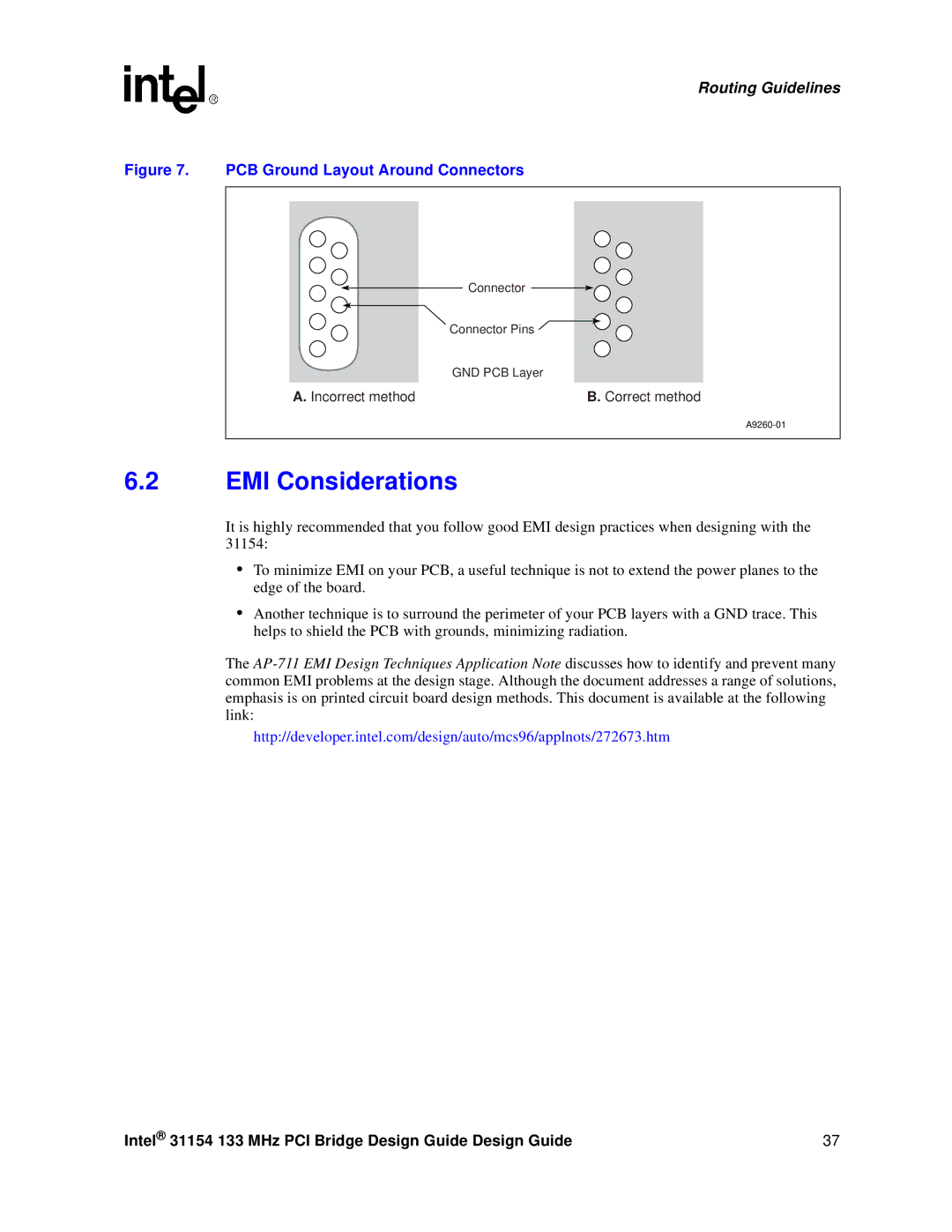
Figure 7. PCB Ground Layout Around Connectors
Connector
Connector Pins ![]()
![]()
GND PCB Layer
A. Incorrect method | B. Correct method |
6.2EMI Considerations
It is highly recommended that you follow good EMI design practices when designing with the 31154:
•To minimize EMI on your PCB, a useful technique is not to extend the power planes to the edge of the board.
•Another technique is to surround the perimeter of your PCB layers with a GND trace. This helps to shield the PCB with grounds, minimizing radiation.
The
http://developer.intel.com/design/auto/mcs96/applnots/272673.htm
Intel® 31154 133 MHz PCI Bridge Design Guide Design Guide | 37 |
