5.3.3Secondary IDSEL Masking
The 31154 supports private devices through the use of IDSEL masking. When the IDSEL_MASK pin is sampled as 1b on the trailing edge of P_RST#, the default value for the Secondary IDSEL Select Register (SISR) is 001Fh to mask devices
5.3.4Secondary Clock Control
The 31154 can disable its secondary clock outputs individually or globally. The straps S_CLKOEN[3:0] determine the number of S_CLKO[8:0] outputs that are enabled. The S_BRCLKO output is dedicated for the bridge feedback clock and cannot be individually disabled.
When the global clock output enable S_GCLKOEN is sampled as 0b, all secondary clock outputs are disabled, and an external clock source is required. The 31154 Bridge still drives the
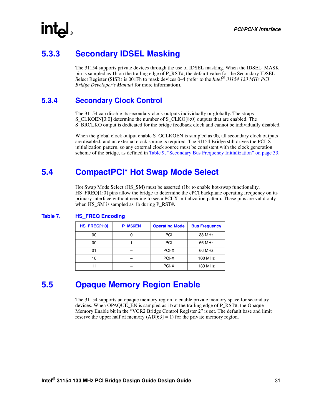
5.4CompactPCI* Hot Swap Mode Select
Hot Swap Mode Select (HS_SM) must be asserted (1b) to enable
HS_FREQ[1:0] pins allow the bridge to determine the cPCI backplane operating frequency on its primary interface without needing to see a
Table 7. | HS_FREQ Encoding |
|
| |
|
|
|
|
|
| HS_FREQ[1:0] | P_M66EN | Operating Mode | Bus Frequency |
|
|
|
|
|
| 00 | 0 | PCI | 33 MHz |
|
|
|
|
|
| 00 | 1 | PCI | 66 MHz |
|
|
|
|
|
| 01 | – |
| 66 MHz |
|
|
|
|
|
| 10 | – |
| 100 MHz |
|
|
|
|
|
| 11 | – |
| 133 MHz |
|
|
|
|
|
5.5Opaque Memory Region Enable
The 31154 supports an opaque memory region to enable private memory space for secondary devices. When OPAQUE_EN is sampled as 1b at the trailing edge of P_RST#, the Opaque Memory Enable bit in the “VCR2 Bridge Control Register 2” is set. The default base and limit reserve the upper half of memory (AD[63] = 1) for the private memory region.
Intel® 31154 133 MHz PCI Bridge Design Guide Design Guide | 31 |