| |
| 7 |
|
|
For acceptable signal integrity with bus speeds up to 133 MHz, it is important for the PCB design layout to have controlled impedance.
The list below provides general guidelines for routing your PCI bus signals:
•Avoid routing signal traces longer than 8".
•All clock nets must be on the top layer.
•All
•All
•P_CLK from the PCI edge finger must be 2.5" ± 0.1".
•P_RST# from the PCI edge finger must be no longer than 3.0" and no shorter than 0.75".
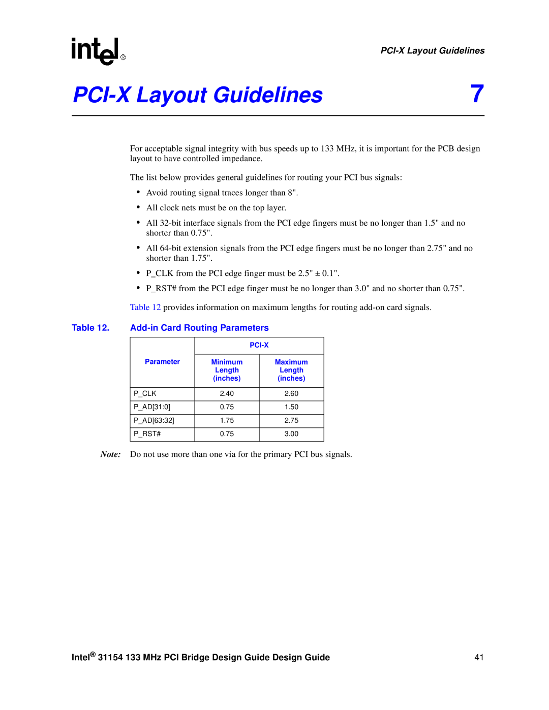
Table 12 provides information on maximum lengths for routing
Table 12. |
|
| ||
|
|
|
|
|
|
|
| ||
| Parameter |
|
| |
| Minimum |
| Maximum | |
|
| Length |
| Length |
|
| (inches) |
| (inches) |
|
|
|
|
|
| P_CLK | 2.40 |
| 2.60 |
|
|
|
|
|
| P_AD[31:0] | 0.75 |
| 1.50 |
|
|
|
|
|
| P_AD[63:32] | 1.75 |
| 2.75 |
|
|
|
|
|
| P_RST# | 0.75 |
| 3.00 |
|
|
|
|
|
Note: Do not use more than one via for the primary PCI bus signals.
Intel® 31154 133 MHz PCI Bridge Design Guide Design Guide | 41 |