|
|
|
|
| Terminations |
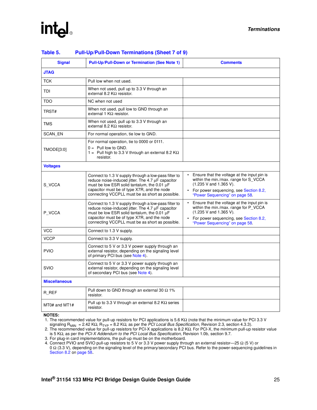
Table 5. |
|
|
| ||
|
|
|
|
|
|
Signal |
|
|
| Comments | |
|
|
|
|
|
|
JTAG |
|
|
|
|
|
|
|
|
|
|
|
TCK |
| Pull low when not used. |
|
|
|
|
|
|
|
|
|
TDI |
| When not used, pull up to 3.3 V through an |
|
|
|
| external 8.2 KΩ resistor. |
|
|
| |
|
|
|
|
| |
|
|
|
|
|
|
TDO |
| NC when not used |
|
|
|
|
|
|
|
|
|
TRST# |
| When not used, pull low to GND through an |
|
|
|
| external 1 KΩ resistor. |
|
|
| |
|
|
|
|
| |
|
|
|
|
|
|
TMS |
| When not used, pull up to 3.3 V through an |
|
|
|
| external 8.2 KΩ resistor. |
|
|
| |
|
|
|
|
| |
|
|
|
|
|
|
SCAN_EN |
| For normal operation, tie low to GND. |
|
|
|
|
|
|
|
|
|
|
| For normal operation, tie to 0000 or 0111. |
|
|
|
TMODE[3:0] |
| 0 = Pull low to GND. |
|
|
|
| 1 = Pull high to 3.3 V through an external 8.2 KΩ |
|
|
| |
|
|
|
|
| |
|
| resistor. |
|
|
|
|
|
|
|
|
|
Voltages |
|
|
|
|
|
|
|
|
|
|
|
|
| Connect to 1.3 V supply through a |
| • | Ensure that the voltage at the input pin is |
|
| reduce |
|
| within the min./max. range for S_VCCA |
S_VCCA |
| must be low ESR solid tantalum, the 0.01 ∝F |
|
| (1.235 V and 1.365 V). |
|
| capacitor must be of type X7R, and the node |
| • | For power sequencing, see Section 8.2, |
|
| connecting VCCPLL must be as short as possible. |
|
| “Power Sequencing” on page 58. |
|
|
|
|
|
|
|
| Connect to 1.3 V supply through a |
| • | Ensure that the voltage at the input pin is |
|
| reduce |
|
| within the min./max. range for P_VCCA |
P_VCCA |
| must be low ESR solid tantalum, the 0.01 ∝F |
|
| (1.235 V and 1.365 V). |
|
| capacitor must be of type X7R, and the node |
| • | For power sequencing, see Section 8.2, |
|
| connecting VCCPLL must be as short as possible. |
|
| “Power Sequencing” on page 58. |
|
|
|
|
|
|
VCC |
| Connect to 1.3 V supply. |
|
|
|
|
|
|
|
|
|
VCCP |
| Connect to 3.3 V supply. |
|
|
|
|
|
|
|
|
|
|
| Connect to 5 V or 3.3 V power supply through an |
|
|
|
PVIO |
| external resistor, depending on the signaling level |
|
|
|
|
| of primary PCI bus (see Note 4). |
|
|
|
|
|
|
|
|
|
|
| Connect to 5 V or 3.3 V power supply through an |
|
|
|
SVIO |
| external resistor, depending on the signaling level |
|
|
|
|
| of secondary PCI bus (see Note 4). |
|
|
|
|
|
|
|
|
|
Miscellaneous |
|
|
|
|
|
|
|
|
|
|
|
R_REF |
| Pull down to GND through an external 30 Ω 1% |
|
|
|
| resistor. |
|
|
| |
|
|
|
|
| |
|
|
|
|
|
|
MT0# and MT1# |
| Pull up to 3.3 V through an external 8.2 KΩ series |
|
|
|
| resistor. |
|
|
| |
|
|
|
|
| |
|
|
|
|
|
|
NOTES:
1.The recommended value for
2.The recommended value for
3.For
4.Connect PVIO and SVIO
0 Ω (3.3 V), depending on the signaling level of the primary/secondary PCI bus. Refer to the
Intel® 31154 133 MHz PCI Bridge Design Guide Design Guide | 25 |