Routing Guidelines
6.1Crosstalk
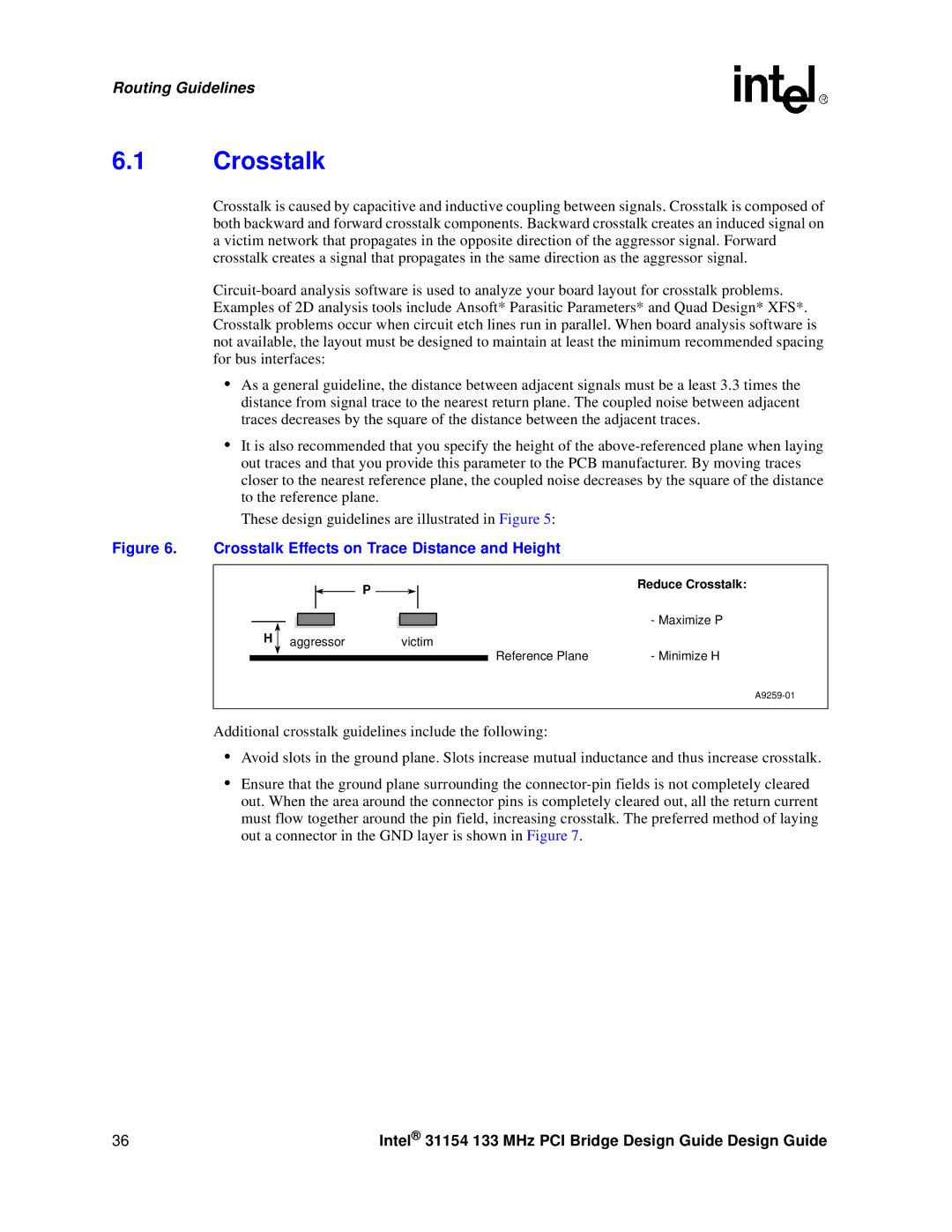
Crosstalk is caused by capacitive and inductive coupling between signals. Crosstalk is composed of both backward and forward crosstalk components. Backward crosstalk creates an induced signal on a victim network that propagates in the opposite direction of the aggressor signal. Forward crosstalk creates a signal that propagates in the same direction as the aggressor signal.
•As a general guideline, the distance between adjacent signals must be a least 3.3 times the distance from signal trace to the nearest return plane. The coupled noise between adjacent traces decreases by the square of the distance between the adjacent traces.
•It is also recommended that you specify the height of the
These design guidelines are illustrated in Figure 5:
Figure 6. Crosstalk Effects on Trace Distance and Height
H
|
|
|
| P |
|
| Reduce Crosstalk: | |
|
|
|
|
|
| |||
|
|
|
|
|
| |||
|
|
|
|
|
|
|
| - Maximize P |
|
|
|
|
|
|
|
| |
|
|
|
|
|
|
|
| |
|
|
|
|
|
|
|
|
|
aggressor |
| victim | - Minimize H | |||||
|
|
|
|
|
|
| Reference Plane | |
Additional crosstalk guidelines include the following:
•Avoid slots in the ground plane. Slots increase mutual inductance and thus increase crosstalk.
•Ensure that the ground plane surrounding the
36 | Intel® 31154 133 MHz PCI Bridge Design Guide Design Guide |