Connectors
VMEbus P1 & P2 Connector Pin Assignments (SBC Mode)
The VMEbus connector P1 provides power and VME signals for
Row B of connector P2 provides power to the MVME5100 and to the upper 8 VMEbus address lines and additional 16 VMEbus data lines.
Rows A, C, Z, and D provide power and interface signals to the5 MVME712 or MVME761 transition module in SBC mode (also called 761
mode and IPMC mode).
It is important to note that the PMC I/O routing to row D and Z are not the same as MVME2600/2700. The PMC I/O routing for row D and row Z is the same as the PMC mode with the exception of pins Z1, 3, 5, 7, 9, 11, 13, 15, and 17 which are used for extended SCSI.
Note A PMC card installed in slot 2 of an MVME5100 in SBC mode MUST NOT connect to
The pin assignments for the P2 connector using the IPMC761 or the
IPMC712 are listed in the following two tables:
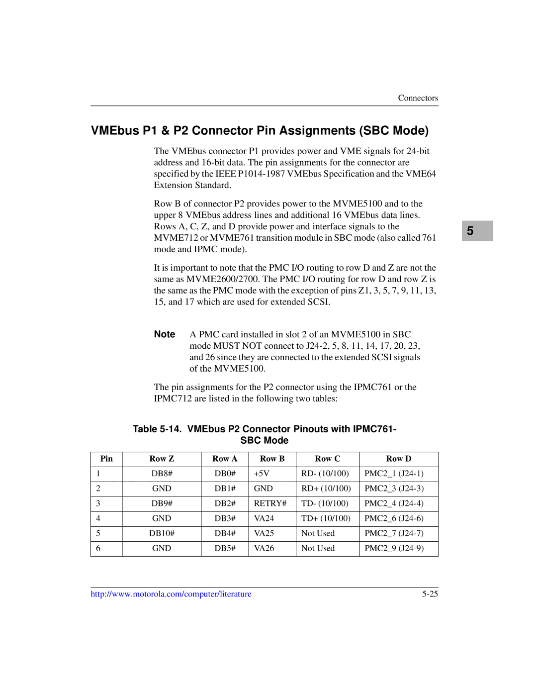
Table 5-14. VMEbus P2 Connector Pinouts with IPMC761-
SBC Mode
Pin | Row Z | Row A | Row B | Row C | Row D |
|
|
|
|
|
|
1 | DB8# | DB0# | +5V | RD- (10/100) | PMC2_1 |
|
|
|
|
|
|
2 | GND | DB1# | GND | RD+ (10/100) | PMC2_3 |
|
|
|
|
|
|
3 | DB9# | DB2# | RETRY# | TD- (10/100) | PMC2_4 |
|
|
|
|
|
|
4 | GND | DB3# | VA24 | TD+ (10/100) | PMC2_6 |
|
|
|
|
|
|
5 | DB10# | DB4# | VA25 | Not Used | PMC2_7 |
|
|
|
|
|
|
6 | GND | DB5# | VA26 | Not Used | PMC2_9 |
|
|
|
|
|
|
http://www.motorola.com/computer/literature |