D |
Functional Description
A, |
|
|
|
|
|
|
|
|
|
|
|
|
BA, |
| DQMB0 |
|
| DQ, |
|
| SCL A0_SPD CLK1,2 | ||||
WE_L, |
|
|
| CKD |
|
| SDA | |||||
| CS_C_L |
|
|
|
| |||||||
RAS_L, |
|
|
|
|
|
|
|
|
|
|
| |
|
|
|
|
|
|
|
|
|
|
|
| |
CAS_L, |
|
|
|
|
|
|
|
|
|
|
|
|
|
|
|
|
|
|
|
|
|
|
|
| |
|
|
|
|
|
|
|
|
|
|
|
|
|
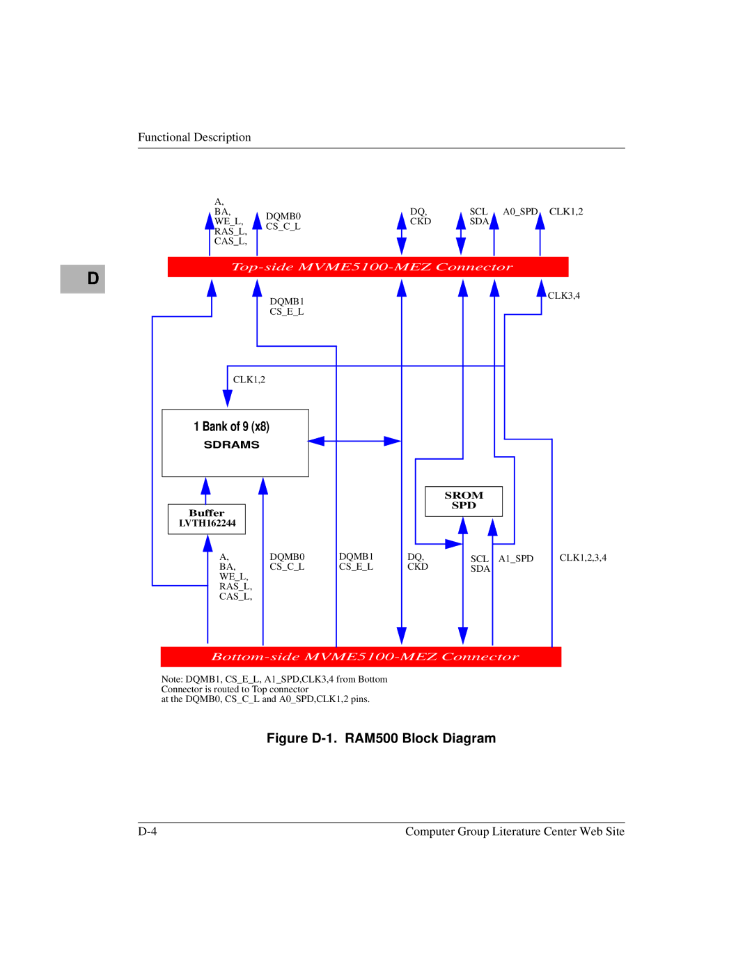
Top-side MVME5100-MEZ Connector
| DQMB1 |
|
|
|
| CLK3,4 |
|
|
|
|
|
| |
| CS_E_L |
|
|
|
|
|
CLK1,2 |
|
|
|
|
|
|
1 Bank of 9 (x8) |
|
|
|
|
|
|
SDRAMS |
|
|
|
|
|
|
|
|
|
| SROM |
|
|
Buffer |
|
|
| SPD |
|
|
|
|
|
|
|
| |
LVTH162244 |
|
|
|
|
|
|
A, | DQMB0 | DQMB1 | DQ, | SCL | A1_SPD | CLK1,2,3,4 |
BA, | CS_C_L | CS_E_L | CKD | SDA |
|
|
WE_L, |
|
|
|
|
|
|
RAS_L, |
|
|
|
|
|
|
CAS_L, |
|
|
|
|
|
|
Note: DQMB1, CS_E_L, A1_SPD,CLK3,4 from Bottom Connector is routed to Top connector
at the DQMB0, CS_C_L and A0_SPD,CLK1,2 pins.
Figure D-1. RAM500 Block Diagram
Computer Group Literature Center Web Site |