D |
RAM500 Connectors
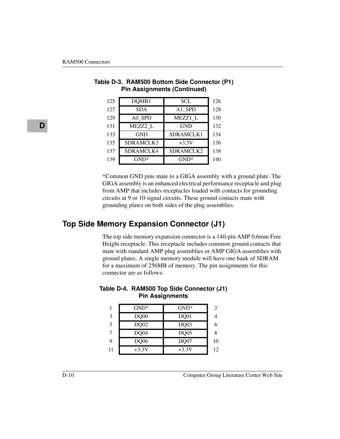
Table D-3. RAM500 Bottom Side Connector (P1)
Pin Assignments (Continued)
125 | DQMB1 | SCL | 126 |
127 |
|
| 128 |
SDA | A1_SPD | ||
129 |
|
| 130 |
A0_SPD | MEZZ1_L | ||
131 |
|
| 132 |
MEZZ2_L | GND | ||
|
|
|
|
133 | GND | SDRAMCLK1 | 134 |
135 |
|
| 136 |
SDRAMCLK3 | +3.3V | ||
137 |
|
| 138 |
SDRAMCLK4 | SDRAMCLK2 | ||
139 |
|
| 140 |
GND* | GND* | ||
|
|
|
|
*Common GND pins mate to a GIGA assembly with a ground plate. The GIGA assembly is an enhanced electrical performance receptacle and plug from AMP that includes receptacles loaded with contacts for grounding circuits at 9 or 10 signal circuits. These ground contacts mate with grounding plates on both sides of the plug assemblies.
Top Side Memory Expansion Connector (J1)
The top side memory expansion connector is a
Table D-4. RAM500 Top Side Connector (J1)
Pin Assignments
1 | GND* | GND* | 2 |
3 |
|
| 4 |
DQ00 | DQ01 | ||
5 |
|
| 6 |
DQ02 | DQ03 | ||
7 |
|
| 8 |
DQ04 | DQ05 | ||
9 |
|
| 10 |
DQ06 | DQ07 | ||
11 |
|
| 12 |
+3.3V | +3.3V | ||
|
|
|
|
Computer Group Literature Center Web Site |
