INSTALLATION PROCEDURE
Figure 4-6 PLO Pin Assignments for Receiving Clock (1-IMG System)
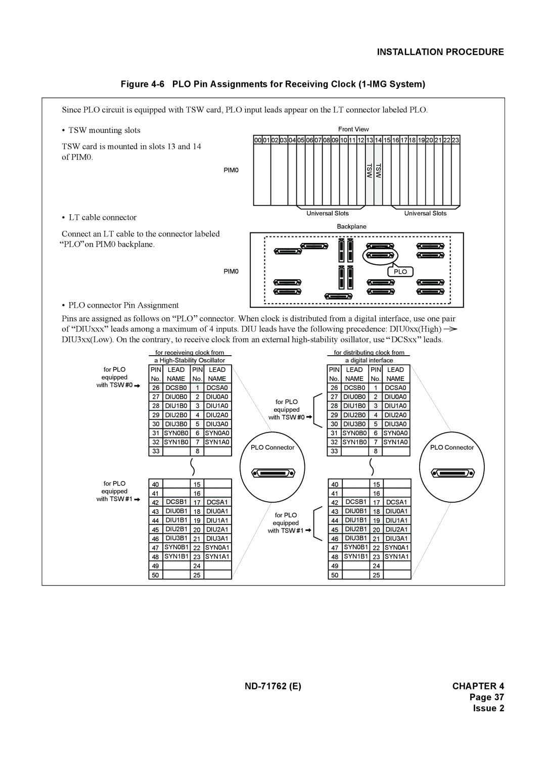
Since PLO circuit is equipped with TSW card, PLO input leads appear on the LT connector labeled PLO.
![]() TSW mounting slots
TSW mounting slots
TSW card is mounted in slots 13 and 14 of PIM0.
PIM0
Front View
00 01 02 03 04 05 06 07 08 09 10 11 12 13 14 15 16 17 18 19 20 21 22 23
TSW
TSW
![]() LT cable connector
LT cable connector
Connect an LT cable to the connector labeled ![]() PLO
PLO![]() on PIM0 backplane.
on PIM0 backplane.
![]() PLO connector Pin Assignment
PLO connector Pin Assignment
Universal Slots | Universal Slots |
Backplane |
|
PIM0 | PLO |
Pins are assigned as follows on ![]() PLO
PLO![]() connector. When clock is distributed from a digital interface, use one pair of
connector. When clock is distributed from a digital interface, use one pair of ![]() DIUxxx
DIUxxx![]() leads among a maximum of 4 inputs. DIU leads have the following precedence: DIU0xx(High)
leads among a maximum of 4 inputs. DIU leads have the following precedence: DIU0xx(High) ![]() DIU3xx(Low). On the contrary, to receive clock from an external
DIU3xx(Low). On the contrary, to receive clock from an external ![]() DCSxx
DCSxx![]() leads.
leads.
for PLO
equipped
with TSW #0 ![]()
for receiveing clock from
a
PIN LEAD PIN LEAD No. NAME No. NAME
26 DCSB0 1 DCSA0
27 DIU0B0 2 DIU0A0
28 DIU1B0 3 DIU1A0
29 DIU2B0 4 DIU2A0
30 DIU3B0 5 DIU3A0
31 SYN0B0 6 SYN0A0
32 SYN1B0 7 SYN1A0
33 8
for distributing clock from
a digital interface
| PIN | LEAD | PIN | LEAD |
|
| No. | NAME | No. | NAME |
|
| 26 | DCSB0 | 1 | DCSA0 |
|
for PLO | 27 | DIU0B0 | 2 | DIU0A0 |
|
28 | DIU1B0 | 3 | DIU1A0 |
| |
equipped |
| ||||
29 | DIU2B0 | 4 | DIU2A0 |
| |
with TSW #0 |
| ||||
| 30 | DIU3B0 | 5 | DIU3A0 |
|
| 31 | SYN0B0 | 6 | SYN0A0 |
|
PLO Connector | 32 | SYN1B0 | 7 | SYN1A0 | PLO Connector |
33 |
| 8 |
| ||
|
|
|
|
for PLO
equipped
with TSW #1 ![]()
4015
4116
42DCSB1 17 DCSA1
43DIU0B1 18 DIU0A1
44DIU1B1 19 DIU1A1
45DIU2B1 20 DIU2A1
46DIU3B1 21 DIU3A1
47SYN0B1 22 SYN0A1
48SYN1B1 23 SYN1A1
4924
5025
for PLO
equipped
with TSW #1 ![]()
4015
4116
42DCSB1 17 DCSA1
43DIU0B1 18 DIU0A1
44DIU1B1 19 DIU1A1
45DIU2B1 20 DIU2A1
46DIU3B1 21 DIU3A1
47SYN0B1 22 SYN0A1
48SYN1B1 23 SYN1A1
4924
5025
Page 37
Issue 2