INSTALLATION PROCEDURE
Figure 4-7 PLO Pin Assignment for Receiving Clock (4-IMG System)
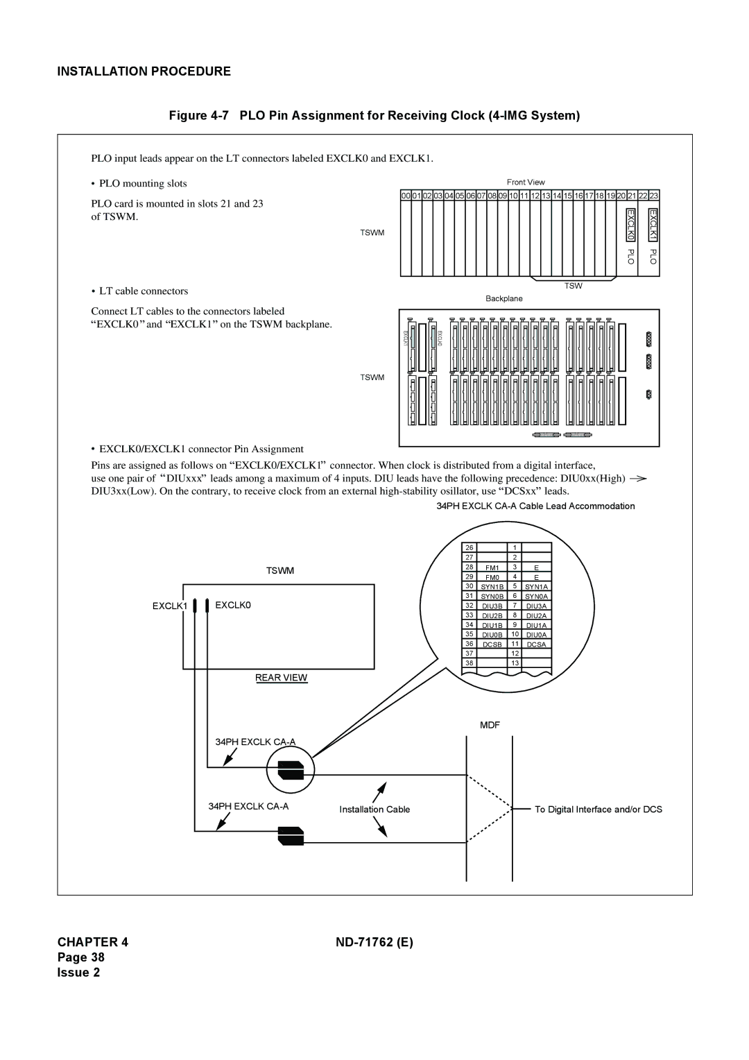
PLO input leads appear on the LT connectors labeled EXCLK0 and EXCLK1.
![]() PLO mounting slots
PLO mounting slots
PLO card is mounted in slots 21 and 23 of TSWM.
TSWM
![]() LT cable connectors
LT cable connectors
Connect LT cables to the connectors labeled ![]() EXCLK0
EXCLK0 ![]() and
and ![]() EXCLK1
EXCLK1![]() on the TSWM backplane.
on the TSWM backplane.
Front View
00 01 02 03 04 05 06 07 08 09 10 11 12 13 14 15 16 17 18 19 20 21 22 23
EXCLK0 |
| EXCLK1 |
PLO |
| PLO |
TSW
Backplane
EXCLK1 |
|
|
|
|
|
|
| EXCLK0 | |
|
|
|
|
|
| ||||
|
| ||||||||
|
| ||||||||
|
|
|
|
|
|
|
|
|
|
|
|
|
|
|
|
|
|
|
|
|
|
|
|
|
|
|
|
|
|
TSWM
![]() EXCLK0/EXCLK1 connector Pin Assignment
EXCLK0/EXCLK1 connector Pin Assignment
Pins are assigned as follows on ![]() EXCLK0/EXCLK1
EXCLK0/EXCLK1![]() connector. When clock is distributed from a digital interface,
connector. When clock is distributed from a digital interface,
use one pair of ![]() DIUxxx
DIUxxx![]() leads among a maximum of 4 inputs. DIU leads have the following precedence: DIU0xx(High)
leads among a maximum of 4 inputs. DIU leads have the following precedence: DIU0xx(High) ![]() DIU3xx(Low). On the contrary, to receive clock from an external
DIU3xx(Low). On the contrary, to receive clock from an external ![]() DCSxx
DCSxx![]() leads.
leads.
34PH EXCLK
EXCLK1 ![]()
![]()
|
|
|
| 26 |
| 1 |
|
|
| |||
|
|
|
|
| 27 |
| 2 |
|
|
| ||
| TSWM |
| 28 | FM1 | 3 |
| E |
| ||||
| 29 | FM0 | 4 |
| E |
| ||||||
|
|
|
|
| ||||||||
|
|
|
|
| 30 | SYN1B | 5 | SYN1A |
| |||
| EXCLK0 |
| 31 | SYN0B | 6 | SYN0A |
| |||||
|
| 32 | DIU3B | 7 | DIU3A |
| ||||||
|
|
|
|
| 33 | DIU2B | 8 | DIU2A |
| |||
|
|
|
|
| 34 | DIU1B | 9 | DIU1A |
| |||
|
|
|
|
| 35 | DIU0B | 10 | DIU0A |
| |||
|
|
|
|
| 36 | DCSB | 11 | DCSA | ||||
|
|
|
|
| 37 |
| 12 |
|
|
| ||
|
|
|
|
| 38 |
| 13 |
|
|
| ||
| REAR VIEW |
|
|
| MDF |
|
|
|
|
| ||
|
|
|
|
|
|
|
|
|
|
|
| |
| 34PH EXCLK |
|
|
|
|
|
|
|
|
| ||
|
|
|
|
|
|
|
|
|
|
|
| |
|
|
|
|
|
|
|
|
|
|
|
|
|
|
|
|
|
|
|
|
|
|
|
|
|
|
| 34PH EXCLK | Installation Cable |
|
|
|
| To Digital Interface and/or DCS | |||||
|
|
|
| |||||||||
|
|
|
|
|
|
|
|
|
|
|
|
|
|
|
|
|
|
|
|
|
|
|
|
|
|
|
|
|
|
|
|
|
|
|
|
|
|
|
CHAPTER 4 |
|
Page 38
Issue 2