IXP1200 Network Processor Family ATM
•Upon reception of the first cell, data11 is saved in the VC cache/table entry. Upon reception of the 2nd cell, data11 is retrieved from the VC cache/table entry, combined with data0 of the second cell, and written in a single burst to DRAM.
Moving the nth cell (not cell0) in a PDU from the RFIFO to DRAM is similar to using the macro atm_move_cell0_rfifo_to_sdram(), except that:
•The nth cell must start with a
•The nth cell must combine data11 of the previous cell with data0, as shown in Figure 17.
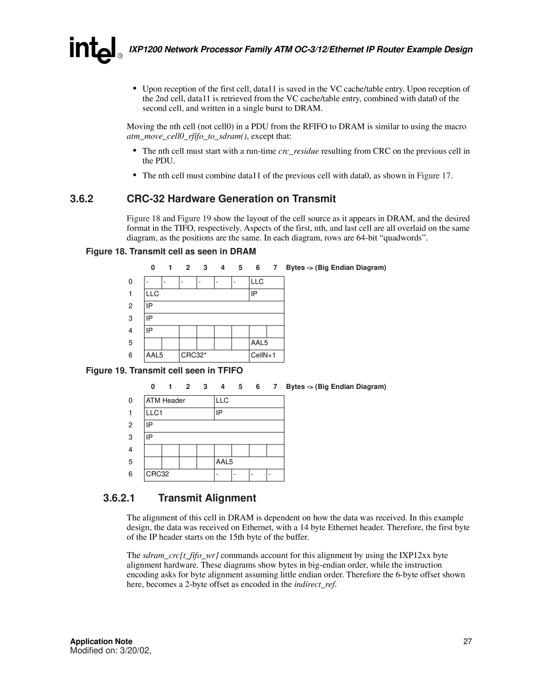
3.6.2CRC-32 Hardware Generation on Transmit
Figure 18 and Figure 19 show the layout of the cell source as it appears in DRAM, and the desired format in the TIFO, respectively. Aspects of the first, nth, and last cell are all overlaid on the same diagram, as the positions are the same. In each diagram, rows are 64-bit “quadwords”.
Figure 18. Transmit cell as seen in DRAM
| 0 | 1 | 2 | 3 | 4 | 5 | 6 |
| 7 Bytes | |
|
|
|
|
|
|
|
|
|
|
|
0 | - | - | - | - | - | - | LLC |
|
| |
|
|
|
|
|
|
|
|
|
|
|
1 | LLC |
|
|
|
|
| IP |
|
| |
|
|
|
|
|
|
|
|
|
|
|
2 | IP |
|
|
|
|
|
|
|
|
|
|
|
|
|
|
|
|
|
|
|
|
3 | IP |
|
|
|
|
|
|
|
|
|
|
|
|
|
|
|
|
|
|
|
|
4 | IP |
|
|
|
|
|
|
|
|
|
|
|
|
|
|
|
|
|
|
|
|
5 |
|
|
|
|
|
| AAL5 |
|
| |
|
|
|
|
|
|
|
|
|
| |
6 | AAL5 |
| CRC32* |
|
| CellN+1 |
| |||
|
|
|
|
|
|
|
|
|
|
|
Figure 19. Transmit cell seen in TFIFO
| 0 1 2 | 3 4 |
| 5 | 6 | 7 Bytes | ||||
|
|
|
|
|
|
|
|
|
|
|
0 | ATM Header |
| LLC |
|
|
|
| |||
|
|
|
|
|
|
|
| |||
1 | LLC1 |
| IP |
|
|
|
| |||
|
|
|
|
|
|
|
|
| ||
2 | IP |
|
|
|
|
|
|
| ||
|
|
|
|
|
|
|
|
| ||
3 | IP |
|
|
|
|
|
|
| ||
4 |
|
|
|
|
|
|
|
|
|
|
|
|
|
|
|
|
|
|
|
| |
|
|
|
|
|
|
|
|
|
|
|
5 |
|
|
|
| AAL5 |
|
|
|
| |
|
|
|
|
|
|
|
|
|
|
|
6 | CRC32 |
| - |
| - | - | - |
| ||
|
|
|
|
|
|
|
|
|
|
|
3.6.2.1Transmit Alignment
The alignment of this cell in DRAM is dependent on how the data was received. In this example design, the data was received on Ethernet, with a 14 byte Ethernet header. Therefore, the first byte of the IP header starts on the 15th byte of the buffer.
The sdram_crc[t_fifo_wr] commands account for this alignment by using the IXP12xx byte alignment hardware. These diagrams show bytes in
Application Note | 27 |
Modified on: 3/20/02,