Intel Server Board SE7520JR2
Revision
Revision History Intel Server Board SE7520JR2
C78844-002
Date Revision Modifications Number
Intel Server Board SE7520JR2 Disclaimers
Iii
Table of Contents
RTC
Intel Server Board SE7520JR2 Table of Contents
System Bios
Table of Contents Intel Server Board SE7520JR2
113
Vii
Platform Management
Viii C78844-002
149
Error Reporting and Handling
201
175
202
Design and Environmental Specifications
216
FCC USA
222
Appendix a Integration and Usage Tips 221
225
Xii Revision C78844-002
Xiii
Intel Server Board SE7520JR2 List of Figures
Xiv
List of Tables Intel Server Board SE7520JR2
Intel Server Board SE7520JR2 List of Tables
Xvi
Xvii
Xviii Revision C78844-002
This page intentionally left blank
Chapter Outline
Intel Server Board SE7520JR2 Introduction
Revision C78844-002
Introduction Intel Server Board SE7520JR2
Server Board Use Disclaimer
Server Board SE7520JR2 SKU Availability
Server Board SE7520JR2 Feature Set
Server Board Overview Intel Server Board SE7520JR2
SE7520JR2 Board Layout Revision C78844-002
32 33
Ref # Description
Server Board Dimensions Revision C78844-002
Functional Architecture Intel Server Board SE7520JR2
Server Board SE7520JR2 Block Diagram Revision C78844-002
Processor Sub-system
Reset Configuration Logic
Processor Voltage Regulators
Processor Module Presence Detection
Processor Support
Common Enabling Kit CEK Design Support
Processor Support Matrix
Processor Family FSB Frequency Support
Processor Mis-population Detection
Jumperless Processor Speed Settings
Mixed Processor Steppings
Mixed Processor Models
Multiple Processor Initialization
CPU Thermal Sensors
Intel E7520 Chipset
Processor Thermal Control Sensor
Processor Thermal Trip Shutdown
Front Side Bus FSB
Memory Controller Hub MCH
MCH Memory Sub-System Overview
PCI Express
Hub Interface
PCI-X Hub PXH
Full-height Riser Slot
Low Profile Riser Slot
2.3 I/OxAPIC Controller
3 I/O Controller Hub ICH5-R
SMBus Interface
PCI Interface
Low Pin Count LPC Interface
Sata Controller
Advanced Programmable Interrupt Controller Apic
Enhanced Power Management
Universal Serial Bus USB Controller
3.8 RTC
Memory Sizing
Memory Sub-System
Memory Population
1GB 2GB
1GB 2GB 4GB
DDR2 400 Dimm population rules are as follows
DDR-266 & DDR-333 Dimm population rules are as follows
Supported DDR-266 Dimm Populations
Supported DDR-333 Dimm Populations
Memory Test
ECC Memory Initialization
Memory Feature On-board Professional Advanced
Memory Monitoring
Memory Monitoring Support by Server Management Level
Memory Rasum Features
Dram ECC Intel x4 Single Device Data Correction x4 Sddc
Integrated Memory Scrub Engine
Integrated Memory Initialization Engine
Retry on Uncorrectable Error
Dimm Sparing Function
Memory Mirroring
Four Dimm Memory Mirror Configuration
Dimm
I/O Sub-System
PCI Subsystem
Logging Memory RAS Information to the SEL
1.2 P64-A and P64-B 64-bit, 100MHz PCI Subsystem
1.1 P32-A 32-bit, 33-MHz PCI Subsystem
1.3 P64-Express Dual x4 PCI Bus Segment
PCI Riser Slots
PCI Bus Numbering
PCI Scan Order
Device Number and Idsel Mapping
PCI Device
Bus# / Device# / Function#
PCAD28
Interrupt Routing
Split Option ROM
Apic Interrupt Routing
PCI Interrupt Routing/Sharing
Interrupt
Legacy Interrupt Sources
Serialized IRQ Support
Interrupt Definitions
ICH5-R PXH Ioapic PCI-E Interface
IRQ Scan for Pciirq
Interface
Intr
IRQ
PCI Interrupt Mapping Diagram
4.1.1 53C1030 Summary of Features
Scsi Support
4.1 LSI* 53C1030 Dual Channel Ultra320 Scsi Controller
Revision C78844-002
Zero Channel RAID
IDE Support
Sata Support
Ultra ATA/100
IDE Initialization
Sata RAID
Video Support
Intel RAID Technology Option ROM
Video Modes
Video Memory Interface
Signal Name Type Description
Video Memory Interface
Column Address Select
Enabled
Network Interface Controller NIC
Dual video
USB 2.0 Support
NIC Connector and Status LEDs
Super I/O Chip
GPIOs
GPIOE11/XA10
Zzbiosrolling GPIOE45/LED2
GPIOE12/XA9
XBUSA9 GPIOE13/XA8
Serial Port a
Serial Ports
Serial Port B
Serial Port Multiplexer Logic
BMC
Rear RJ45 Serial B Port Configuration
Removable Media Drives
Bios Flash
Floppy Disk Support
Keyboard and Mouse Support
Configuration and Initialization
Memory Space
1MB
DOS Compatibility Region Revision C78844-002
DOS Compatibility Region
Extended System Bios
Add-in Card Bios and Buffer Area
System Bios
DOS Area
Extended Memory Map Revision C78844-002
Extended Memory
1.2.5 I/O Apic Configuration Space
High Bios
Main Memory
PCI Memory Space
Global Enable High Enable Tseg Enable Compatible High H
System Management Mode Handling
SMM Space Table
Range
2 I/O Map
O Map
Address es Resource
Revision
Accessing Configuration Space
Clock Generation and Distribution
Configaddress Register
System Bios Intel Server Board SE7520JR2
Bios Identification String
Bios Power On Self Test Post
Flash Architecture and Flash Update Utility
Intel Server Board SE7520JR2 System Bios
User Interface
Splash Screen/Diagnostic Window
System Diagnostic Screen
System Activity Window
Bios Boot Popup Menu
Quiet Boot / OEM Splash Screen
Post Activity Window
Bios Setup Keyboard Command Bar Options
Bios Setup Utility
Please select boot device
Localization
Entering Bios Setup
Bios Setup, Main Menu Options
Main Menu
Bios Setup, Advanced Menu Options
Advanced Menu
English
Bios Setup, Processor Configuration Sub-menu Options
Processor Configuration Sub-menu
Disabled
CPU Cpuid
Bios Setup IDE Configuration Menu Options
IDE Configuration Sub-menu
Both
A1-3rdM/A2-4thM
Mixed P-ATA-S-ATA Configuration with only Primary P-ATA
Host & Device
ATA M-S
Cdrom Armd
Auto
SWDMA0-0
SWDMA0-1
Super I/O Configuration Sub-menu
Floppy Configuration Sub-menu
Bios Setup, Floppy Configuration Sub-menu Selections
Bios Setup, Super I/O Configuration Sub-menu
USB Mass Storage Device Configuration Sub-menu
USB Configuration Sub-menu
Bios Setup, USB Configuration Sub-menu Selections
HiSpeed
Bios Setup, PCI Configuration Sub-menu Selections
PCI Configuration Sub-menu
Bios Setup, Memory Configuration Sub-menu Selections
Memory Configuration Sub-menu
Bios Setup, Boot Menu Selections
Boot Menu
Dimm 3A
Dimm 3B
Bios Setup, Boot Settings Configuration Sub-menu Selections
Boot Settings Configuration Sub-menu Selections
This is
Off
2.3.3 Hard Disk Drive Sub-menu Selections
Boot Device Priority Sub-menu Selections
2.3.4 Removable Drive Sub-menu Selections
2.3.5 Atapi Cdrom drives sub-menu selections
Security Menu
Bios Setup, Security Menu Options
Limited
Minute
Disable BSP
Bios Setup, Server Menu Selections
Server Menu
Stays Off
System Management Sub-menu Selections
Bios Setup, System Management Sub-menu Selections
100 C78844-002
Stay On
Event Log Configuration Sub-menu Selections
Serial Console Features Sub-menu Selections
Bios Setup, Serial Console Features Sub-menu Selections
Bios Setup, Event Log Configuration Sub-menu Selections
Bios Setup, Exit Menu Selections
Rolling Bios and On-line Updates
Feature Options Help Text
Exit Menu
Flash Bios
Flash Update Utility
Recovery Mode
User Binary Area
Configuration Reset
Bios Recovery
104 Revision C78844-002
OEM Binary
Security
Revision 105 C78844-002
Security Features Operating Model
Operating Model
106 Revision C78844-002
Scenario #2
Scenario #1
Scenario #3
107
Password Clear Jumper
Operating System Boot, Sleep, and Wake
Extensible Firmware Interface EFI
EFI Shell
Advanced Configuration and Power Interface Acpi
Sleep and Wake Functionality
Revision 109 C78844-002
On to Off OS absent
Power Switch Off to On
On to Off OS present
On to Sleep Acpi
Sleep to On Acpi
System Sleep States
C78844-002 111
PXE Bios Support
Console Redirection
112 Revision C78844-002
Suppoted Management Features by Tier
Revision 113 C78844-002
Intel Management
114 Revision C78844-002
Platform Management Intel Server Board SE7520JR2
PC87427
Platform Management Architecture Overview
Ipmi Messaging, Commands, and Abstractions
1 5V Standby
116 Revision C78844-002
Revision 117 C78844-002
Ipmi ‘Sensor Model’
Private Management Busses
Management Controllers
118 Revision C78844-002
Revision 119 C78844-002
120 Revision C78844-002
Revision 121 C78844-002
On-Board Platform Management Features and Functionality
Server Management I2C Buses
Power Control Interfaces
External Interface to the mBMC
Server Management I2C Bus ID Assignments
Revision 123 C78844-002
MBMC Hardware Architecture
124 Revision C78844-002
Power Supply Interface Signals
Revision 125 C78844-002
Power Supply Control Signals
Power-up Sequence
Power Control Sources
Power-down Sequence
System Reset Control
Control Panel System Reset
Reset Control Sources
Power button assertion
Reset button assertion
Control Panel Indicators
Combined power and reset button assertion
Power LED
SSI Power LED Operation
Non-Critical Condition
Fault / Status LED
Degraded Condition
Chassis ID LED
Reset Button
Power Button
Diagnostic Interrupt Button Control Panel NMI
Chassis Intrusion
Watchdog Timer
Secure Mode Operation
Baseboard Fan Control
MBMC Peripheral SMBus
SEL Erasure
Sensor Data Record SDR Repository
Timestamp Clock
Initialization Agent
NMI Generation
Field Replaceable Unit FRU Inventory Devices
SMI Generation
Event Message Reception
Messaging Interfaces
MBMC Self Test
LAN Channel Capacity
LAN Interface
Revision 135 C78844-002
LAN Channel Capability Options
Event Filtering and Alerting
Platform Event Filtering PEF
136 Revision C78844-002
MBMC Sensor Support
Action Priority Delayed Type
Alert over LAN
PEF Action Priorities
Platform Sensors for On-Board Platform Instrumentation
138 Revision C78844-002
Event Readable
Sensor # Event Event Offset Assert Readable
Revision 139 C78844-002
Sensor Name Reading Event Data Record Type Triggers
Value/Offsets Action Type
140 Revision C78844-002
Ierr
ID LED
Revision 141 C78844-002
142
IMM BMC Sensor Support
Number Type Triggers Deassert Offsets
Sensor Event Event Offset Assert Readable
143 C78844-002
Intel Server Board SE7520JR2 Platform Management
144
Lvds Scsi
OEM
FRB1, FRB2
FRB3
Dimm
VRM
Wired For Management WFM
System Management Bios Smbios
Vital Product Data VPD
Intel Server Board SE7520JR2 Error Reporting and Handling
Fault Resilient Booting FRB
1 FRB1 BSP Self-Test Failures
2 FRB2 BSP Post Failures
OS Watchdog Timer Operating System Load Failures
3 FRB3 BSP Reset Failures
Error Reporting and Handling Intel Server Board SE7520JR2
150 Revision C78844-002
AP Failures
Treatment of Failed Processors
Revision 151 C78844-002
Memory Error Handling
Memory Error Handling in RAS Mode
152 Revision C78844-002
Memory Error Handling in non-RAS Mode
Memory Error Handling mBMC vs Sahalee
Revision 153 C78844-002
Memory Error Handling in non-RAS mode
Single-bit ECC Error Throttling Prevention
Dimm Enabling
154 Revision C78844-002
PCI Bus Error
Error Logging
Processor Bus Error
SMI Handler
Error Messages and Error Codes
Storage Device Bios Messages
Boot Bios Messages
157 C78844-002
No ROM Basic
158
159 C78844-002
System Configuration Bios Messages
Virus Related Bios Messages
160
Eprom
Miscellaneous Bios Messages
Cmos Bios Messages
USB Bios Error Messages
161 C78844-002
Smbios Bios Error Messages
Post Error Codes
Error Codes and Messages
Error Code Error Message Response
C78844-002 163
0146 Insufficient Memory to Shadow PCI ROM Pause
Error Codes Sent to the Management Module
Error code Error messages
164
Bios Generated Beep Codes
Bios Generated Post Error Beep Codes
Revision 165 C78844-002
Number of Beeps Description
Boot Block Error Beep Codes
Boot Block Error Beep Codes
Number of Beeps Troubleshooting Action
BMC Generated Beep Codes Professional/Advanced only
Diagnostic LEDs
System ROM Bios Post Task Test Point Port 80h Code
Checkpoints
Post Progress Code LED Example
Post Code Checkpoints
Diagnostic LEDs
Back edge of baseboard
Post Code Checkpoints
169 C78844-002
Bootblock Initialization Code Checkpoints
Bootblock Initialization Code Checkpoints
170 Revision C78844-002
Cmos
Bootblock Recovery Code Checkpoint
Bootblock Recovery Code Checkpoint
171 C78844-002
DIM Code Checkpoints
DIM Code Checkpoints
172 Revision C78844-002
Checkpoint Description
Memory Error Codes
Acpi Runtime Checkpoints
Post Progress Fifo Professional / Advanced only
174 Revision C78844-002
Light Guided Diagnostics
Intel Server Board SE7520JR2 Connectors and Jumper Blocks
Power Connectors
Power Connector Pin-out
12V Power Connector J4J1
Riser Slots
IDE Power Connector Pinout U2E1
Low Profile PCI-X Riser Slot
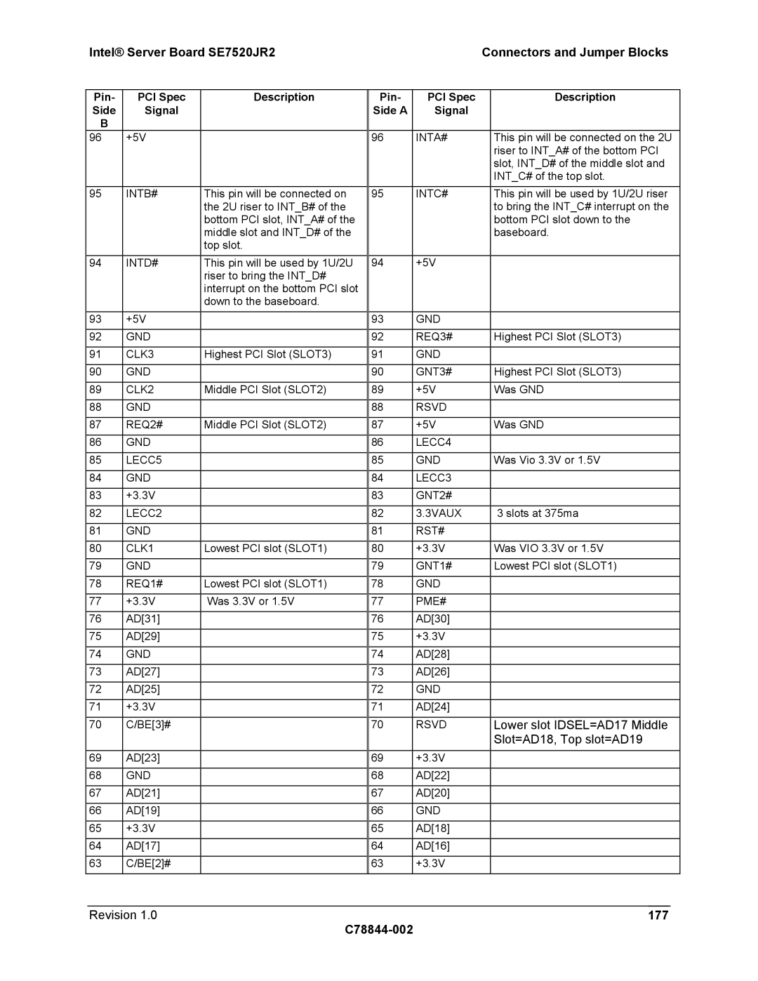
Low Profile Riser Slot Pinout
Pin PCI Spec Description Side Signal
Pin PCI Spec Description Side a Signal
Revision 177 C78844-002
178 Revision C78844-002
Connectors and Jumper Blocks Intel Server Board SE7520JR2
Full Height PCI-X Riser Slot
Pin connector length = 139.45mm=5.49
Revision 179 C78844-002
Prsntn
180 Revision C78844-002
Pin-Side PCI Spec Description Signal
REFCLK2
Perstn
Revision 181 C78844-002
182 Revision C78844-002
Revision 183 C78844-002
PAR64
Pxhrst
IMM Connector Pinout J1C1
Intel Management Module Connector
System Management Headers
184 Revision C78844-002
Description Pin
C78844-002 185
186 C78844-002
Icmb Header
Pin Signal Name Type Description
Ipmb Header
Icmb Header Pin-out J1D1
188 Revision C78844-002
Pin Signal Name Description
OEM RMC Connector J3B2
Control Panel Connectors
OEM RMC Connector Pinout J3B2
Pin Signal Name
190 Revision C78844-002
Pin# Signal Name Pin #
Revision 191 C78844-002
Control Panel SSI Standard 34-Pin Header Pin-out
P5V P5VSTBY
P5VSTBY Fpidledl FPSTATUSLED1R Fpidbtnl GND Fphddfltledr
VGA Connector
I/O Connectors
VGA Connector Pin-out
192
Scsi Connectors
NIC Connectors
RJ-45 10/100/1000 NIC Connector Pin-out
Internal/External 68-pin Vhdci Scsi Connector Pin-out
ATA-100 40-pin Connector Pin-out J3K1
ATA-100 Connector
Pin# Signal Name
Signal Name Pin#
Floppy Controller Connector
Sata Connectors
Sata Connector Pin-out J1H1 and J1H5
Revision 195 C78844-002
External RJ-45 Serial B Port Pin-out
Serial Port Connectors
Internal 9-pin Serial a Header Pin-out J1A3
196 Revision C78844-002
USB Connector
Keyboard and Mouse Connector
External USB Connector Pin-out
Stacked PS/2 Keyboard and Mouse Port Pin-out
Internal 2x5 USB Connector J1G1
Internal 1x10 USB Connector Pin-out J1F1
Fan Headers
198 Revision C78844-002
CPU1/CPU2 Fan Connector Pin-out J5F2, J7F1
Intel Server Chassis Fan Header Pin-out J3K6
Revision 199 C78844-002
Misc. Headers and Connectors
Chassis Intrusion Header
Hard Drive Activity LED Header
Jumper Blocks
Settings
Jumper Block Definitions
Revision 201 C78844-002
Power Supply Requirements
Server Board SE7520JR2 Design Specification
Output Connectors
Board Design Specifications
Revision 203 C78844-002
Power Harness Specification Drawing
P2 Processor Power Connector
P1 Main Power Connector
P1 Main Power Connector
P2 Processor Power Connector
P4 Peripheral Connectors
P3 Power Signal Connector
P7 Hard Drive Back Plane Power Connector
Grounding
Remote Sense
Standby Outputs
206 Revision C78844-002
Dynamic Loading
Voltage Regulation
Voltage Regulation Limits
Transient Load Requirements
Capacitive Loading
Common Mode Noise
Closed Loop Stability
Ripple / Noise
Zero Load Stability Requirements
Soft Starting
Timing Requirements
Output Voltage Timing
1500
210 Revision C78844-002
2500
100 1000
Revision 211 C78844-002
Residual Voltage Immunity in Standby Mode
Product Regulatory Compliance
Product Safety Compliance
Product EMC Compliance Class a Compliance
212 Revision C78844-002
Product Regulatory Compliance Markings
Certifications / Registrations / Declarations
Product Certification Markings
Revision 213 C78844-002
FCC USA
Electromagnetic Compatibility Notices
Industry Canada ICES-003
214 Revision C78844-002
Taiwan Declaration of Conformity Bsmi
Europe CE Declaration of Conformity
Korean Compliance RRL
Revision 215 C78844-002
Updating the System Software
Programming FRU and SDR Data
216 Revision C78844-002
Cmos Clear using Control Panel
Cmos Clear Using J1H2 Jumper Block
Clearing Cmos
Revision 217 C78844-002
218 Revision C78844-002
Bios Recovery Operation
Revision 219 C78844-002
Page
Revision 221 C78844-002
Appendix a Integration and Usage Tips
Glossary Intel Server Board SE7520JR2
222
Term Definition
C78844-002 223
Intel Server Board SE7520JR2 Glossary
224 Revision C78844-002
Revision 225 C78844-002
Intel Server Board SE7520JR2 Reference Documents