KFM2G16Q2A KFN4G16Q2A
Initial issue Jul
Revision No History
Revision No
Nand
Flash Product Type Selector
PKG
NOR
Ordering Information
Architectural Benefits
Device Performance
Product Features
Device Architecture
System Hardware
General Overview
Definitions
Error Correction Code
Detailed Product Description
Pin Configuration
1 2Gb Product KFM2G16Q2A
2 4Gb Product KFN4G16Q2A
Pin Description
Internal Nand Array Memory Organization
Block Diagram
Memory Array Organization
OTP
Internal Memory Array Information Area Block Sector
Internal Memory Array Organization
External BufferRAM Memory Organization
External BufferRAM Memory
Internal Nand Array Memory
Total Size 1KB+32B 2KB+64B
BootRAM DataRAM
BootRAM DataRAM0 DataRAM1 Main area data
BootRAM
Memory Map
Block Block Address Sector Size
Block Block Address
0082h 0000h~00FFh 128KB Block162
0080h 0000h~00FFh 128KB Block160
0081h 0000h~00FFh 128KB Block161
0083h 0000h~00FFh 128KB Block163
00E1h 0000h~00FFh 128KB Block194 00C2h
Block192 00C0h 0000h~00FFh 128KB
00E0h 0000h~00FFh 128KB Block193 00C1h
00E2h 0000h~00FFh 128KB Block195 00C3h
0102h 0000h~00FFh 128KB Block290 0122h
0100h 0000h~00FFh 128KB Block288 0120h
0101h 0000h~00FFh 128KB Block289 0121h
0103h 0000h~00FFh 128KB Block291 0123h
0142h 0000h~00FFh 128KB Block354 0162h
0140h 0000h~00FFh 128KB Block352 0160h
0141h 0000h~00FFh 128KB Block353 0161h
0143h 0000h~00FFh 128KB Block355 0163h
0000h~00FFh 128KB Block386 0182h Block418
Block384 0180h 0000h~00FFh 128KB Block416
0000h~00FFh 128KB Block385 0181h Block417
0000h~00FFh 128KB Block387 0183h Block419
01C1h 0000h~00FFh 128KB
01C0h 0000h~00FFh 128KB
01E0h 0000h~00FFh 128KB
01E1h 0000h~00FFh 128KB
0202h 0000h~00FFh 128KB Block546 0222h
0200h 0000h~00FFh 128KB Block544 0220h
0201h 0000h~00FFh 128KB Block545 0221h
0203h 0000h~00FFh 128KB Block547 0223h
0242h 0000h~00FFh 128KB Block610 0262h
0240h 0000h~00FFh 128KB Block608 0260h
0241h 0000h~00FFh 128KB Block609 0261h
0243h 0000h~00FFh 128KB
0282h 0000h~00FFh 128KB Block674
0280h 0000h~00FFh 128KB Block672
0281h 0000h~00FFh 128KB Block673
0283h 0000h~00FFh 128KB Block675
02E1h 0000h~00FFh 128KB Block706 02C2h
Block704 02C0h 0000h~00FFh 128KB
02E0h 0000h~00FFh 128KB Block705 02C1h
02E2h 0000h~00FFh 128KB Block707 02C3h
0302h 0000h~00FFh 128KB Block802 0322h
0300h 0000h~00FFh 128KB Block800 0320h
0301h 0000h~00FFh 128KB Block801 0321h
0303h 0000h~00FFh 128KB Block803 0323h
0342h 0000h~00FFh 128KB Block866 0362h
0340h 0000h~00FFh 128KB Block864 0360h
0341h 0000h~00FFh 128KB Block865 0361h
0343h 0000h~00FFh 128KB Block867 0363h
0000h~00FFh 128KB Block898 0382h Block930
Block896 0380h 0000h~00FFh 128KB Block928
0000h~00FFh 128KB Block897 0381h Block929
0000h~00FFh 128KB Block899 0383h Block931
03C1h 0000h~00FFh 128KB
03C0h 0000h~00FFh 128KB
03E0h 0000h~00FFh 128KB
03E1h 0000h~00FFh 128KB
0402h 0000h~00FFh 128KB Block1058 0422h
0400h 0000h~00FFh 128KB Block1056 0420h
0401h 0000h~00FFh 128KB Block1057 0421h
0403h 0000h~00FFh 128KB Block1059 0423h
0441h 0000h~00FFh 128KB
0440h 0000h~00FFh 128KB
0460h 0000h~00FFh 128KB
0461h 0000h~00FFh 128KB
0482h 0000h~00FFh 128KB
0480h 0000h~00FFh 128KB
0481h 0000h~00FFh 128KB
0483h 0000h~00FFh 128KB
04C2h 0000h~00FFh 128KB Block1250 04E2h
04C0h 0000h~00FFh 128KB Block1248 04E0h
04C1h 0000h~00FFh 128KB Block1249 04E1h
04C3h 0000h~00FFh 128KB Block1251 04E3h
0502h 0000h~00FFh 128KB Block1314 0522h
0500h 0000h~00FFh 128KB Block1312 0520h
0501h 0000h~00FFh 128KB Block1313 0521h
0503h 0000h~00FFh 128KB Block1315 0523h
0542h 0000h~00FFh 128KB Block1378 0562h
0540h 0000h~00FFh 128KB Block1376 0560h
0541h 0000h~00FFh 128KB Block1377 0561h
0543h 0000h~00FFh 128KB Block1379 0563h
0582h 0000h~00FFh 128KB Block1442
0580h 0000h~00FFh 128KB Block1440
0581h 0000h~00FFh 128KB Block1441
0583h 0000h~00FFh 128KB Block1443
05C2h 0000h~00FFh 128KB Block1506 05E2h
05C0h 0000h~00FFh 128KB Block1504 05E0h
05C1h 0000h~00FFh 128KB Block1505 05E1h
05C3h 0000h~00FFh 128KB Block1507 05E3h
0602h 0000h~00FFh 128KB Block1570 0622h
0600h 0000h~00FFh 128KB Block1568 0620h
0601h 0000h~00FFh 128KB Block1569 0621h
0603h 0000h~00FFh 128KB Block1571 0623h
0642h 0000h~00FFh 128KB Block1634 0662h
0640h 0000h~00FFh 128KB Block1632 0660h
0641h 0000h~00FFh 128KB Block1633 0661h
0643h 0000h~00FFh 128KB Block1635 0663h
0682h 0000h~00FFh 128KB Block1698
0680h 0000h~00FFh 128KB Block1696
0681h 0000h~00FFh 128KB Block1697
0683h 0000h~00FFh 128KB Block1699
06C2h 0000h~00FFh 128KB Block1762 06E2h
06C0h 0000h~00FFh 128KB Block1760 06E0h
06C1h 0000h~00FFh 128KB Block1761 06E1h
06C3h 0000h~00FFh 128KB Block1763 06E3h
0702h 0000h~00FFh 128KB Block1826 0722h
0700h 0000h~00FFh 128KB Block1824 0720h
0701h 0000h~00FFh 128KB Block1825 0721h
0703h 0000h~00FFh 128KB Block1827 0723h
0742h 0000h~00FFh 128KB Block1890 0762h
0740h 0000h~00FFh 128KB Block1888 0760h
0741h 0000h~00FFh 128KB Block1889 0761h
0743h 0000h~00FFh 128KB Block1891 0763h
0000h~00FFh 128KB Block1922 0782h Block1954
Block1920 0780h 0000h~00FFh 128KB Block1952
0000h~00FFh 128KB Block1921 0781h Block1953
0000h~00FFh 128KB Block1923 0783h Block1955
07C2h 0000h~00FFh 128KB Block2018 07E2h
07C0h 0000h~00FFh 128KB Block2016 07E0h
07C1h 0000h~00FFh 128KB Block2017 07E1h
07C3h 0000h~00FFh 128KB Block2019 07E3h
Lnternal Memory Spare Area Assignment
Word Byte
External Memory BufferRAM Address Map
Division Address Size Usage Description
8048h~804Fh16B
External Memory Map Detail Information
0800h~08FFh512B 0900h~09FFh512B DataM
External Memory Spare Area Assignment
Buf
8027h 1004Eh
Managed by Internal ECC logic DataS 8023h 10046h
ECC Code for Main area data 3rd 8026h 1004Ch
8028h 10050h 8029h 10052h Managed by Internal ECC logic
8049h
Buf Word Byte
8048h
Managed by Internal ECC logic
Address Name Host Description
Registers
Register Address Map
Manufacturer ID Register F000h R
Device Identification Description
Device ID Default
Device ID Register F001h R
DeviceID150
Data Buffer Size Register F003h R
F003h, default = 0800h DataBufSize
Version ID Register F002h
This Register is reserved for internal use
Technology Register F006h R
Boot Buffer Size Register F004h R
Number of Buffers Register F005h R
Start Address1 Register F100h R/W
Start Address2 Register F101h R/W
Fcba
Start Address3 Register F102h R/W
Start Address4 Register F103h R/W
Fcpa FCSA1
Start Address7 Register F106h
Start Address5 Register F104h R/W
Start Address6 Register F105h
Start Address8 Register F107h R/W
BSC
Start Buffer Register F200h R/W
BSA
CMD
Command Register F220h R/W
Acceptable
Operation
Interrupt Register
Two Methods to Clear Interrupt Register in Command Input
Write command into INT will automatically
System Configuration 1 Register F221h R, R/W
Brwl
RDY Polarity RDYpol Information7
Burst Length BL
Burst Length BL Information119 Definition Description
INT Polarity INTpol Information6
Iobe
MRSMode register Setting Description Mode Description
Write Mode WM
Write Mode Information1 Definition
Bwps
System Configuration 2 Register F222h
Controller Status Register F240h R
Error Information10 Sector/Page Load/Program/CopyBack
= ready default
Error
Program
Otpbl
Rstb
Otpl
Plane2 Current
Plane1 Current
Plane2 Previous
Time Out to
Controller Status Register Output Modes
Flash Memory
Rsti
Interrupt Status Register F241h R/W
INT
Reset Interrupt Rsti
Default State Valid
EI Interrupt Status Conditions Default State Valid
Rsti Interrupt Status Conditions Default State Valid
Nand Flash Write Protection Status Register F24Eh R
Start Block Address Register F24Ch R/W
End Block Address Register F24Dh
SBA
ERm3 ERs3 ERm2 ERs2 ERm1 ERs1 ERm0 ERs01
Error Status ERm, ERs ECC Status
ECC Status Register FF00h R
ECC Information150
Reserved0000 ECCposWord1 ECCposIO1
Reserved0000 ECCposWord0 ECCposIO0
Reserved0000000000 ECClogSector0 ECCposIO0
Reserved0000000000 ECClogSector1 ECCposIO1
Reserved0000 ECCposWord3 ECCposIO3
Reserved0000 ECCposWord2 ECCposIO2
Reserved0000000000 ECClogSector2 ECCposIO2
Reserved0000000000 ECClogSector3 ECCposIO3
ECClogSector Information Error Position
ECC Log Sector
Add Data 00E0h 0000h3 Read Identification Data XXXXh4 0090h
Command Based Operation
Reset MuxOneNAND Add BP1 Data 00F0h
Read Identification Data Command
Reset MuxOneNAND Command
Load MuxOneNAND Command
Identification Data Description Address Data Out
CLK AVD
Device Bus Operation
Operation ADQ0~15
Reset Mode Operation
Hot Reset Mode Operation
Cold Reset Mode Operation
Warm Reset Mode Operation
Nand Flash Core Reset Mode Operation
Nand Flash Array Write Protection Operation
BootRAM Write Protection Operation
Write Protection Operation
Nand Array Write Protection States
Locked Lock Command Sequence
Unlocked Unlock Command Sequence
Unlocked All Block Unlock Command Sequence
Unlocked Nand Array Write Protection State
Power On
Nand Flash Array Write Protection State Diagram
Locked-tight Lock-Tight Command Sequence
Locked-tight Nand Array Write Protection State
Add F100h DQ=DFS
Data Protection Operation Flow Diagram
Add F101h DQ=DBS
Add F24Ch DQ=SBA
DQ=0027h
All Block Unlock Flow Diagram
Add F241h DQ=0000h
Add F241h DQ15=INT
YES
Data Protection During Power Down Operation
Load Operation
Host reads data from DataRAM Read completed
Read Operation
Asynchronous Read Mode Operation RM=0, WM=0
Synchronous Read Mode Operation RM=1, WM=X
Continuous Linear Burst Read Operation
2.2 4-, 8-, 16-, 32-Word Linear Burst Read Operation
Handshaking Operation
Output Disable Mode Operation
Programmable Burst Read Latency Operation
Cache-Read flow chart is on the following
Cache Read Operation RM=X, WM=X
END
Write ‘Cache Read’ Command Add F220h DQ=000Eh
Write ’DFS*, FBA’ of Flash Add F100h DQ=DFS, FBA
Map out
Cache Read Diagram
1st DQ0 Address A/DQ15 Setting INT 2nd
4th Status Command Host reads 1st
Setting Read Read data from DataRAM Cont
See Timing Diagram 6.3
Synchronous Burst Block Read OperationRM=1, WM=X
Terminating Synchronous Burst Block Read
Synchronous Burst Block Read Boundary
Four Clock Burst Read Latency default condition
102
Synchronous Burst Block Read Operation Flow Chart
103
See Timing Diagram 6.8, 6.9
Synchronous WriteRM=1, WM=1
Program Operation
Addressing for program operation
ADD DP DQ=Data-in
Program Operation Flow Diagram
Program Lock Error Program Error
Add F100h DQ=DFS*’, FBA
11.1 2X Program Operation
107
Add F220h DQ=007Dh
2X Program Operation Flow Diagram
Add F100h DQ=DFS*, FBA
108
11.2 2X Cache Program Operation
109
DBS, DFS is for DDP
110
11.3 2X Interleave Cache Program Operation
111
For a chip
2X Interleave Cache Program Operation Flow Diagram Start
Last 2 Plane PGM For a chip?
112
Copy-Back Program Operation
113
Flash Memory
Copy-Back Program Operation with Random Data Input
115
Erase Operation
Block Erase Operation
Multi-Block Erase Operation
Locked Blocks
Add F220h DQ=0095h
Multi Block Erase/ Multi Block Erase Verify Read Flow Chart
Multi-Block Erase Verify Read Operation
Add F240h DQ10=0
119
Erase Suspend / Erase Resume Operation
Erase Suspend During a Block Erase Operation
OTP Operation
OTP Block Area Structure
1st Block OTP Area Structure
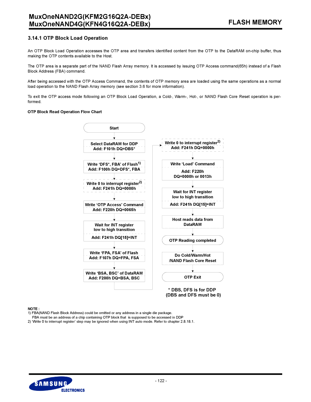
OTP Block Load Operation
122
OTP Block Program Operation
Programming the OTP Area
OTPL=0? YES
OTP Block Program Operation Flow Chart
Write ‘DFS, FBA’ of Flash Add F100h DQ=DFS, FBA3
OTP Lock Operation Steps
OTP Block Lock Operation
Locking the OTP
Write ’DFS, FBA’ of Flash Add F100h DQ=DFS, FBA3
Add F241h DQ15=INT Do Cold reset
Automatically Updated
126
1st Block OTP Lock Operation Steps
14.4 1st Block OTP Lock Operation
Locking the 1st Block OTP
128
OTP and 1st Block OTP simultaneous Lock Operation Steps
OTP and 1st Block OTP Lock Operation
Locking the OTP and 1st Block OTP
130
Write-While-Program Operation
Dual Operations
Read-While-Load Operation
Data Load
DB1
ADQ
DB0
AVD INT
133
DQ6 DQ5~DQ0
16 DQ6 Toggle Bit
Status DQ15~DQ7
Progress Data Loading Don’t Care
ECC Operation
ECC Bypass Operation
Invalid Block Operation
Invalid Block Identification Table Operation
Invalid Block Replacement Operation
Invalid Block Table Creation Flow Chart Start
Block B
Block Replacement Operation Sequence
1st 1th Nth
KFM2G16Q2A
Absolute Maximum Ratings
Operating Conditions
DC Characteristics
Test Conditions
Device Capacitance
Valid Block Characteristics
AC Test Conditions
DDP
Max Min
AC Characteristics for Synchronous Burst Read
66MHz 83MHz Unit
See Timing Diagrams 6.18, 6.19 Parameter Symbol Min Max
AC Characteristics for Asynchronous Read
See Timing Diagrams 6.5, 6.6, 6.22
KFN4G16Q2A
Min Max
AC Characteristics for Asynchronous Write
AC Characteristics for Burst Write Operation
66MHz 83MHz Unit Min
AC Characteristics for Synchronous Burst Block Read
AC Characteristics for Load/Program/Erase Performance
AC Characteristics for INT Auto Mode
CLK
8-Word Linear Burst Read Mode with Wrap Around
Continuous Linear Burst Read Mode with Wrap Around
RDY
147
Synchronous Burst Block Read Timing
148
149
Burst block read
Low
See AC Characteristics Table DQ0 DQ15
Asynchronous Read VA Transition Before
Asynchronous Read VA Transition After AVD Low
Hi-Z
Asynchronous Write
Valid WD
151
≈D7
8-Word Linear Burst Write Mode
Burst Write Operation followed by Burst Read
152
Start Initial Burst Write Operation
153
Load Operation Timing
See AC Characteristics Tables 5.5, 5.7
Load Command Sequence last two cycles Read Data
Bit
Program Operation Timing
155
ADQ0~ADQ15 . . A1
13 2X Program Operation Timing
Ongoing Status
MuxOneNAND2GKFM2G16Q2A MuxOneNAND4GKFN4G16Q2A
14 2X Cache Program
Operation Timing
ADQ0~
15 2X Interleave
Cache Program
ADQ15
159
Erase Command Sequence Read Status Data
Block Erase Operation Timing
Bootcode copy
Cold Reset Timing
Bootcode copy done
Default
CE, OE
Warm Reset Timing
See AC Characteristics Tables
INT bit
BPNote 00F0h Or F220h Or 00F3h
Hot Reset Timing
ADQi
Idle
163
Nand Flash Core Reset Timing
Data Protection Timing During Power Down
164
Status RD Hi-Z
RDY
165
INT auto mode
Write command into Command Register INT will automatically
166
Methods of Determining Interrupt Status
INT Type Mono INT Type DDP
INT Pin to a Host General Purpose I/O
Synchronous Mode Using the INT Pin
Asynchronous Mode Using the INT Pin
168
Handshaking Mode Non-Handshaking Mode
Polling the Interrupt Register Status Bit
Rpohm
INT pol = ‘High’ Default
Determining Rp Value DDP, QDP only
~50k ohm Ready
INT pol = ‘Low’
Vcc or Vccq
Vss KFN4G16Q2A @ Vcc = 1.8V, Ta = 25C , CL = 30pF
Boot Sequence
Boot Sequence
Boot Loaders in MuxOneNAND
Boot Loaders in MuxOneNAND Description
BL1
NBL3 NBL1 NBL2
BL2
BL1 BL2
173
2G product KFM2G16Q2A
4G product KFN4G16Q2A