Sigma DE2-70 manual Using SDRAM/SRAM/Flash

Models: DE2-70

1 93
Download 93 pages 32 Kb
Page 60
Image 60
5.16 Using SDRAM/SRAM/Flash

DE2-70 User Manual

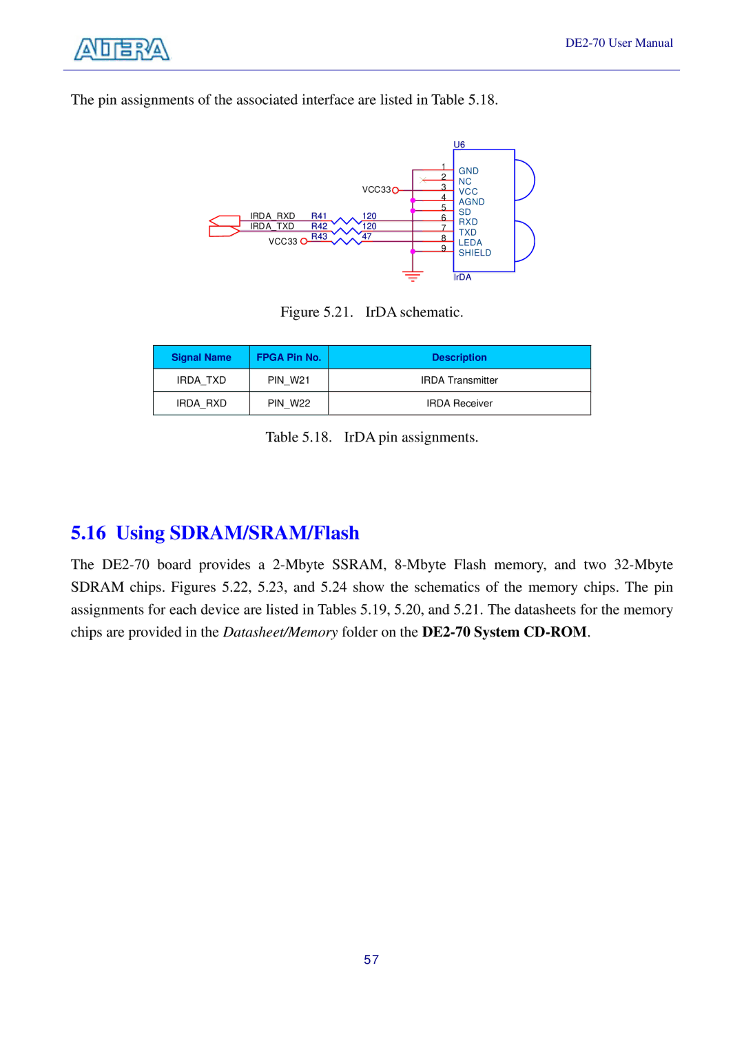
The pin assignments of the associated interface are listed in Table 5.18.


1


2


VCC33

3


4


IRDA_RXD

R41

120

5

6

IRDA_TXD

R42

120

7

VCC33

R43

47

8


9


U6

GND NC VCC AGND SD RXD TXD LEDA SHIELD

IrDA


Figure 5.21.

IrDA schematic.


Signal Name

FPGA Pin No.


Description


IRDA_TXD

PIN_W21


IRDA Transmitter


IRDA_RXD

PIN_W22


IRDA Receiver


Table 5.18. IrDA pin assignments.

5.16 Using SDRAM/SRAM/Flash

The DE2-70 board provides a 2-Mbyte SSRAM, 8-Mbyte Flash memory, and two 32-Mbyte SDRAM chips. Figures 5.22, 5.23, and 5.24 show the schematics of the memory chips. The pin assignments for each device are listed in Tables 5.19, 5.20, and 5.21. The datasheets for the memory chips are provided in the Datasheet/Memory folder on the DE2-70 System CD-ROM.

57

Page 60
Image 60
Sigma DE2-70 manual Using SDRAM/SRAM/Flash