5.7 Using VGA
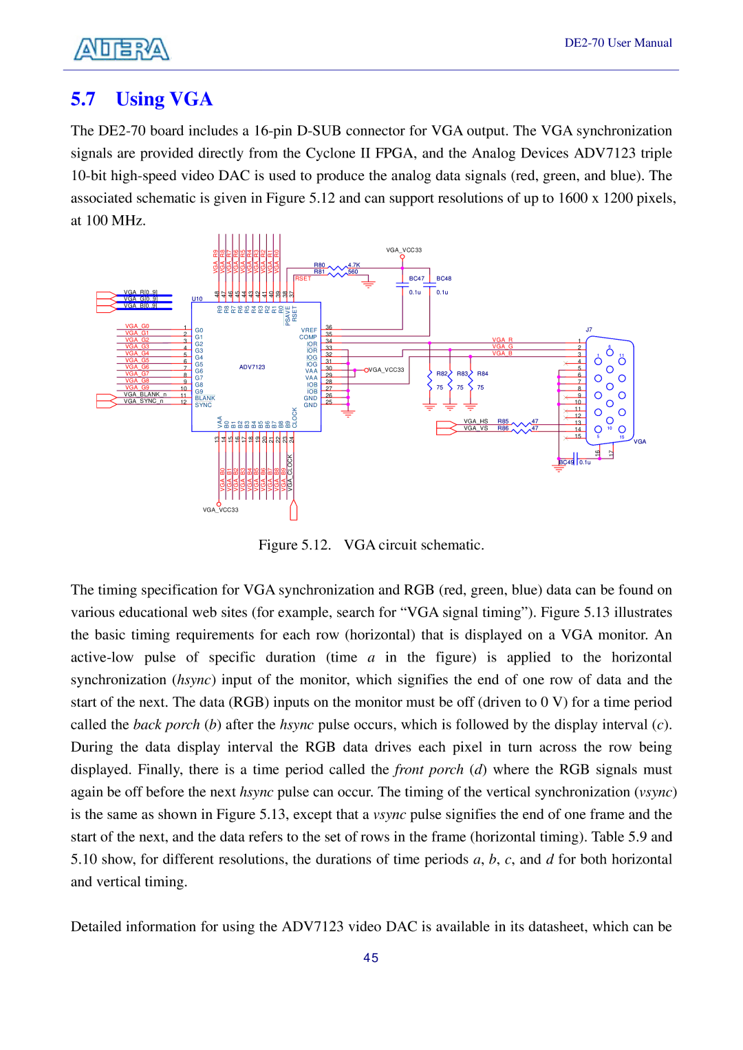
The
VGA_R[0..9] |
|
VGA_G[0..9] |
|
VGA_B[0..9] |
|
VGA_G0 | 1 |
VGA_G1 | 2 |
VGA_G2 | 3 |
VGA_G3 | 4 |
VGA_G4 | 5 |
VGA_G5 | 6 |
VGA_G6 | 7 |
VGA_G7 | 8 |
VGA_G8 | 9 |
VGA_G9 | 10 |
VGA_BLANK_n | 11 |
VGA_SYNC_n | 12 |
|
| 9R_ _ A | 8R A | _ | 7R A | _ | 6R A | _ | 5R A | _ | 4R A | _ | 3R A | _ | 2R A | _ | 1R A | _ | 0R A |
|
|
|
|
| R80 |
| |||
|
|
|
|
|
|
|
|
|
|
|
|
|
|
|
| ||||||||||||||
|
| GV | GV |
| GV |
| GV |
| GV |
| GV |
| GV |
| GV |
| GV |
| GV |
|
|
|
|
|
|
|
| ||
|
|
|
|
|
|
|
|
|
|
|
|
|
|
| R81 |
| |||||||||||||
|
|
|
|
|
|
|
|
|
|
|
|
|
|
|
|
|
|
|
|
|
|
|
|
|
|
| RSET |
|
|
U10 | 48 | 47 |
| 46 |
| 45 |
| 44 |
| 43 |
| 42 |
| 41 |
| 40 |
| 39 |
| 38 |
| 37 |
|
|
| ||||
|
|
|
|
|
|
|
|
|
|
|
|
|
|
|
|
|
|
|
|
|
|
|
|
|
|
|
| ||
|
|
|
|
| |||||||||||||||||||||||||
|
|
| 9R 8R 7R 6R 5R 4R 3R 2R 1R 0R | EVA TES S R |
| ||||||||||||||||||||||||
|
|
|
|
|
|
|
|
|
|
|
|
|
|
|
|
|
|
|
|
|
|
|
| P | 36 | ||||
| G0 |
|
|
|
|
|
|
|
|
|
|
|
|
|
|
|
|
|
|
|
|
|
|
|
|
| VREF |
| |
|
|
|
|
|
|
|
|
|
|
|
|
|
|
|
|
|
|
|
|
|
|
|
|
|
|
| 35 | ||
| G1 |
|
|
|
|
|
|
|
|
|
|
|
|
|
|
|
|
|
|
|
|
|
|
|
|
| COMP |
| |
|
|
|
|
|
|
|
|
|
|
|
|
|
|
|
|
|
|
|
|
|
|
|
|
|
|
| 34 | ||
| G2 |
|
|
|
|
|
|
|
|
|
|
|
|
|
|
|
|
|
|
|
|
|
|
|
|
| IOR |
| |
|
|
|
|
|
|
|
|
|
|
|
|
|
|
|
|
|
|
|
|
|
|
|
|
|
|
| 33 | ||
| G3 |
|
|
|
|
|
|
|
|
|
|
|
|
|
|
|
|
|
|
|
|
|
|
|
|
| IOR |
| |
|
|
|
|
|
|
|
|
|
|
|
|
|
|
|
|
|
|
|
|
|
|
|
|
|
|
| 32 | ||
| G4 |
|
|
|
|
|
|
|
|
|
|
|
|
|
|
|
|
|
|
|
|
|
|
|
|
| IOG |
| |
|
|
|
|
|
|
|
|
|
|
|
|
|
|
|
|
|
|
|
|
|
|
|
|
|
|
| 31 | ||
| G5 |
|
|
|
|
|
|
| ADV7123 |
|
|
|
| IOG |
| ||||||||||||||
|
|
|
|
|
|
|
|
|
|
|
|
| 30 | ||||||||||||||||
| G6 |
|
|
|
|
|
|
|
|
|
|
| VAA |
| |||||||||||||||
|
|
|
|
|
|
|
|
|
|
|
|
|
|
|
|
|
|
|
|
|
|
|
|
|
|
| 29 | ||
| G7 |
|
|
|
|
|
|
|
|
|
|
|
|
|
|
|
|
|
|
|
|
|
|
|
|
| VAA | ||
|
|
|
|
|
|
|
|
|
|
|
|
|
|
|
|
|
|
|
|
|
|
|
|
|
| 28 | |||
| G8 |
|
|
|
|
|
|
|
|
|
|
|
|
|
|
|
|
|
|
|
|
|
|
|
|
| IOB |
| |
|
|
|
|
|
|
|
|
|
|
|
|
|
|
|
|
|
|
|
|
|
|
|
|
|
|
| 27 | ||
| G9 |
|
|
|
|
|
|
|
|
|
|
|
|
|
|
|
|
|
|
|
|
|
|
|
|
| IOB |
| |
|
|
|
|
|
|
|
|
|
|
|
|
|
|
|
|
|
|
|
|
|
|
|
|
|
|
| 26 | ||
| BLANK |
|
|
|
| GND |
| ||||||||||||||||||||||
|
|
|
|
|
| 25 | |||||||||||||||||||||||
| SYNC |
|
|
|
|
|
|
|
|
|
|
|
|
|
|
|
|
|
|
|
|
|
|
|
|
| GND |
| |
|
|
|
|
|
|
|
|
|
|
|
|
|
|
|
|
|
|
|
|
|
|
|
|
|
|
|
| ||
|
|
|
|
|
|
|
|
|
|
|
|
|
|
|
|
|
|
|
|
|
|
|
|
|
| KC |
| ||
|
|
| AA 0 1 2 3 4 5 6 7 8 9 LOC V B B B B B B B B B B |
| |||||||||||||||||||||||||
|
|
|
|
|
|
|
| ||||||||||||||||||||||
|
| 13 | 14 |
| 15 |
| 16 |
| 17 |
| 18 |
| 19 |
| 20 |
| 21 |
| 22 |
| 23 |
| 24 |
|
|
| |||
|
|
|
| 0B |
| 1B |
| 2B |
| 3B |
| 4B |
| 5B |
| 6B |
| 7B |
| 8B |
| 9B |
| KCLO C |
|
|
| ||
|
|
|
|
|
|
|
|
|
|
|
|
|
|
|
|
| |||||||||||||
|
|
|
| _AG V |
| _AG V |
| _AG V |
| _AG V |
| _AG V |
| _AG V |
| _AG V |
| _AG V |
| _AG V |
| _AG V |
| _AG V |
|
|
| ||
|
|
|
|
|
|
|
|
|
|
|
|
|
|
|
|
|
|
|
|
|
|
|
|
|
|
|
|
|
|
VGA_VCC33 |
|
|
|
|
|
4.7K |
|
|
|
|
|
560 |
|
|
|
|
|
BC47 | BC48 |
|
|
|
|
0.1u | 0.1u |
|
|
|
|
|
|
|
| VGA_R |
|
|
|
|
| VGA_G |
|
|
|
|
| VGA_B |
|
VGA_VCC33 | R82 | R83 | R84 |
|
|
|
|
| |||
| 75 | 75 | 75 |
|
|
|
| VGA_HS | R85 | 47 | |
|
| VGA_VS | R86 | 47 | |
| J7 |
| 1 |
| 2 |
| 3 |
| 4 |
| 5 |
| 6 |
| 7 |
| 8 |
| 9 |
| 10 |
| 11 |
| 12 |
| 13 |
| 14 |
| 15 |
BC49 | 0.1u |
1
5 16
6
11
10
15 VGA
17
VGA_VCC33
Figure 5.12. VGA circuit schematic.
The timing specification for VGA synchronization and RGB (red, green, blue) data can be found on various educational web sites (for example, search for “VGA signal timing”). Figure 5.13 illustrates the basic timing requirements for each row (horizontal) that is displayed on a VGA monitor. An
5.10show, for different resolutions, the durations of time periods a, b, c, and d for both horizontal and vertical timing.
Detailed information for using the ADV7123 video DAC is available in its datasheet, which can be
45