GPIO_0 |
| GPIO_1 |
|
|
|
SMA
Connector
4 | |
Oscillator |
|
|
|
TV | |
Oscillator | decoder 1 |
TV
decoder 2
2 | 2 |
2 | 2 |
Cyclone II
FPGA
4 |
2 |
SD Card
AUDIO CODEC
PS/2
Ethernet
VGA
DAC
SDRAM
1
SDRAM
2
SSRAM
FLASH
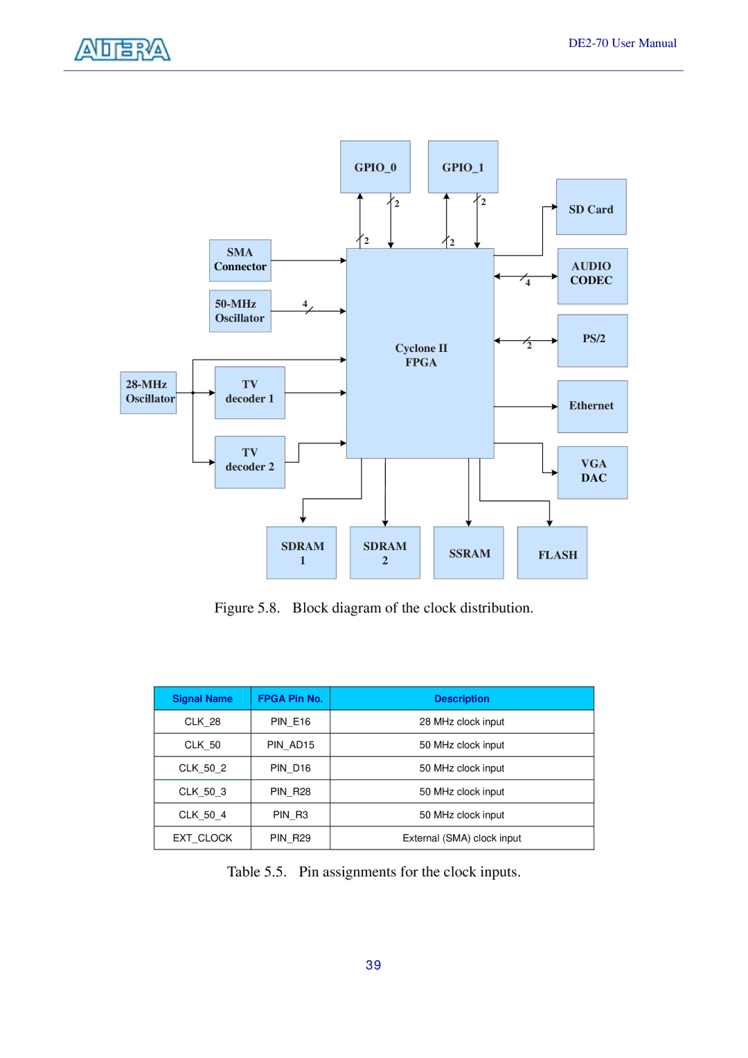
Figure 5.8. Block diagram of the clock distribution.
Signal Name | FPGA Pin No. | Description |
|
|
|
CLK_28 | PIN_E16 | 28 MHz clock input |
|
|
|
CLK_50 | PIN_AD15 | 50 MHz clock input |
|
|
|
CLK_50_2 | PIN_D16 | 50 MHz clock input |
|
|
|
CLK_50_3 | PIN_R28 | 50 MHz clock input |
|
|
|
CLK_50_4 | PIN_R3 | 50 MHz clock input |
|
|
|
EXT_CLOCK | PIN_R29 | External (SMA) clock input |
|
|
|
Table 5.5. Pin assignments for the clock inputs.
39