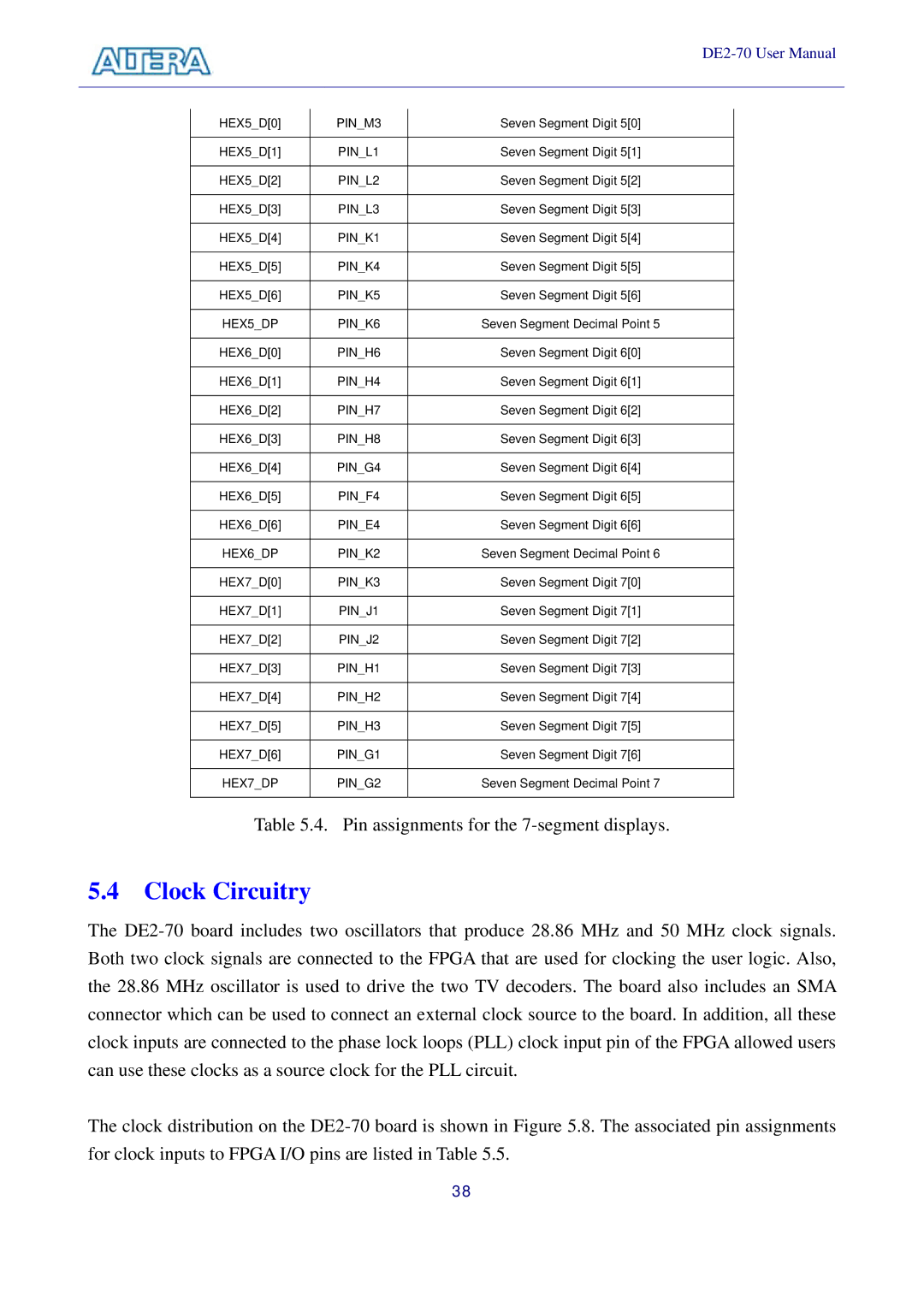
HEX5_D[0] | PIN_M3 | Seven Segment Digit 5[0] |
|
|
|
HEX5_D[1] | PIN_L1 | Seven Segment Digit 5[1] |
|
|
|
HEX5_D[2] | PIN_L2 | Seven Segment Digit 5[2] |
|
|
|
HEX5_D[3] | PIN_L3 | Seven Segment Digit 5[3] |
|
|
|
HEX5_D[4] | PIN_K1 | Seven Segment Digit 5[4] |
|
|
|
HEX5_D[5] | PIN_K4 | Seven Segment Digit 5[5] |
|
|
|
HEX5_D[6] | PIN_K5 | Seven Segment Digit 5[6] |
|
|
|
HEX5_DP | PIN_K6 | Seven Segment Decimal Point 5 |
|
|
|
HEX6_D[0] | PIN_H6 | Seven Segment Digit 6[0] |
|
|
|
HEX6_D[1] | PIN_H4 | Seven Segment Digit 6[1] |
|
|
|
HEX6_D[2] | PIN_H7 | Seven Segment Digit 6[2] |
|
|
|
HEX6_D[3] | PIN_H8 | Seven Segment Digit 6[3] |
|
|
|
HEX6_D[4] | PIN_G4 | Seven Segment Digit 6[4] |
|
|
|
HEX6_D[5] | PIN_F4 | Seven Segment Digit 6[5] |
|
|
|
HEX6_D[6] | PIN_E4 | Seven Segment Digit 6[6] |
|
|
|
HEX6_DP | PIN_K2 | Seven Segment Decimal Point 6 |
|
|
|
HEX7_D[0] | PIN_K3 | Seven Segment Digit 7[0] |
|
|
|
HEX7_D[1] | PIN_J1 | Seven Segment Digit 7[1] |
|
|
|
HEX7_D[2] | PIN_J2 | Seven Segment Digit 7[2] |
|
|
|
HEX7_D[3] | PIN_H1 | Seven Segment Digit 7[3] |
|
|
|
HEX7_D[4] | PIN_H2 | Seven Segment Digit 7[4] |
|
|
|
HEX7_D[5] | PIN_H3 | Seven Segment Digit 7[5] |
|
|
|
HEX7_D[6] | PIN_G1 | Seven Segment Digit 7[6] |
|
|
|
HEX7_DP | PIN_G2 | Seven Segment Decimal Point 7 |
|
|
|
Table 5.4. Pin assignments for the
5.4 Clock Circuitry
The
The clock distribution on the
38