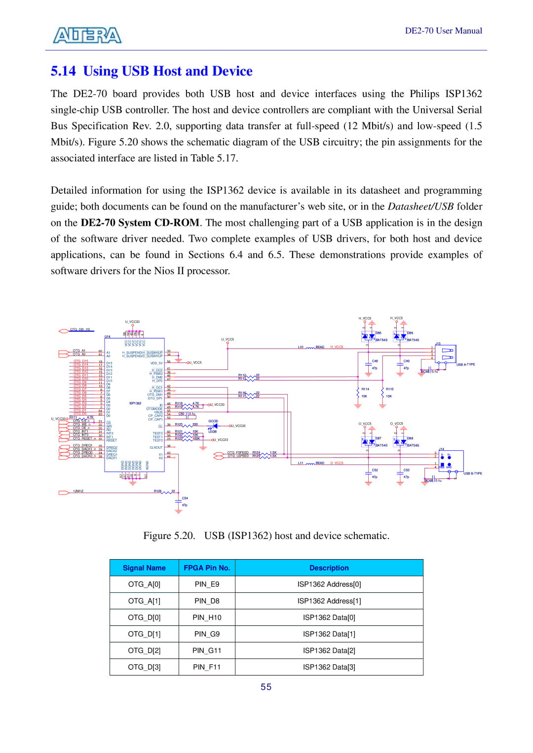
5.14 Using USB Host and Device
The
Detailed information for using the ISP1362 device is available in its datasheet and programming guide; both documents can be found on the manufacturer’s web site, or in the Datasheet/USB folder on the
| OTG_D[0..15] |
| ||
| OTG_A1 |
| 62 | |
| OTG_A0 |
| 61 | |
| OTG_D15 | 18 | ||
| OTG_D14 | 17 | ||
| OTG_D13 | 16 | ||
| OTG_D12 | 15 | ||
| OTG_D11 | 13 | ||
| OTG_D10 | 12 | ||
| OTG_D9 |
| 11 | |
| OTG_D8 |
| 10 | |
| OTG_D7 |
| 8 | |
| OTG_D6 |
| 7 | |
| OTG_D5 |
| 6 | |
| OTG_D4 |
| 5 | |
| OTG_D3 |
| 3 | |
| OTG_D2 |
| 2 | |
| OTG_D1 |
| 64 | |
| OTG_D0 | 4.7K | 63 | |
U_VCC33 | R111 |
| ||
OTG_CS_n | 21 | |||
| ||||
| OTG_WE_n | 22 | ||
| OTG_OE_n | 20 | ||
| OTG_INT1 | 31 | ||
| OTG_INT0 | 30 | ||
| OTG_RESET_n | 32 | ||
| OTG_DREQ1 | 25 | ||
| OTG_DACK1_n | 29 | ||
| OTG_DREQ0 | 24 | ||
| OTG_DACK0_n | 28 | ||
| 12MHZ |
|
| |
|
|
|
|
|
| U_VCC33 |
|
|
|
|
|
|
| ||||||
|
|
|
|
|
|
|
|
|
|
|
|
|
|
|
|
|
|
| |
U14 | 58 | 52 | 40 | 26 | 14 | 4 |
|
|
|
|
|
|
|
| |||||
|
|
|
|
|
| VCC VCC VCC VCC VCC VCC | |||||||||||||
| A1 |
|
|
|
|
|
|
|
| ||||||||||
|
| H_SUSPEND/H_SUSWKUP | |||||||||||||||||
| A0 |
| H_SUSPEND/D_SUSWKUP | ||||||||||||||||
| D15 |
|
|
|
|
|
|
|
|
|
|
| VDD_5V | ||||||
| D14 |
|
|
|
|
|
|
|
|
|
|
|
|
|
|
| |||
| D13 |
|
|
|
|
|
|
|
|
|
|
|
| H_OC2 | |||||
| D12 |
|
|
|
|
|
|
|
|
|
|
| H_PSW2 | ||||||
| D11 |
|
|
|
|
|
|
|
|
|
|
| H_DM2 | ||||||
| D10 |
|
|
|
|
|
|
|
|
|
|
|
| H_DP2 | |||||
| D9 |
|
|
|
|
|
|
|
|
|
|
|
|
|
|
| |||
| D8 |
|
|
|
|
|
|
|
|
|
|
|
| H_OC1 |
| ||||
| D7 |
|
|
|
|
|
|
|
|
|
|
| H_PSW1 | ||||||
| D6 |
|
|
|
|
|
|
|
|
|
| OTG_DM1 | |||||||
| D5 |
|
|
|
|
|
|
|
|
|
| OTG_DP1 | |||||||
| D4 |
|
|
| ISP1362 |
|
|
|
|
|
|
| |||||||
| D3 |
|
|
|
|
|
|
|
| ID | |||||||||
|
|
|
|
|
|
|
|
|
|
|
|
|
| ||||||
| D2 |
|
|
|
|
|
|
|
|
| OTGMODE | ||||||||
| D1 |
|
|
|
|
|
|
|
|
|
|
|
| VBUS | |||||
| D0 |
|
|
|
|
|
|
|
|
|
| CP_CAP2 | |||||||
|
|
|
|
|
|
|
|
|
|
|
|
|
|
| CP_CAP1 | ||||
|
| CS |
|
|
|
|
|
|
|
|
|
|
|
|
|
|
|
|
|
| WR |
|
|
|
|
|
|
|
|
|
|
|
|
| GL | ||||
| RD |
|
|
|
|
|
|
|
|
|
|
|
|
|
|
| |||
| INT2 |
|
|
|
|
|
|
|
|
|
|
|
| TEST2 | |||||
| INT1 |
|
|
|
|
|
|
|
|
|
|
|
|
| TEST1 | ||||
| RESET |
|
|
|
|
|
|
|
|
|
|
|
| TEST0 | |||||
| DREQ2 |
|
|
|
|
|
|
|
|
|
|
| CLKOUT | ||||||
| DACK2 |
|
|
|
|
|
|
|
|
|
|
|
|
|
|
| |||
| DREQ1 |
|
|
|
|
|
|
|
|
|
|
|
|
| X1 | ||||
| DACK1 | DGND DGND DGND DGND ND ND DG DG |
|
|
|
|
| X2 | |||||||||||
|
|
|
|
| NDAG | ||||||||||||||
|
|
|
|
|
|
|
|
|
|
|
|
|
|
|
|
|
|
|
|
|
|
|
|
| 57 | 37 | 27 | 19 | 9 | 1 |
|
| 51 |
|
| R126 | |||
|
|
|
|
|
|
|
|
|
|
|
|
|
|
|
|
| |||
|
|
|
|
|
|
|
|
|
|
|
|
|
|
|
|
| |||
|
|
|
|
|
|
|
|
|
|
|
|
|
|
|
|
|
|
|
|
|
|
|
|
|
|
|
| H_VCC5 | H_VCC5 |
|
|
|
|
| ||
|
|
|
|
|
|
|
| 2 | 1 | 2 | 1 |
|
|
|
|
|
|
|
|
|
|
|
|
|
| D85 |
| D86 |
|
|
|
|
|
|
|
| U_VCC5 |
|
|
|
|
| BAT54S | BAT54S |
| J13 |
|
| ||
|
|
|
|
| L10 | BEAD | H_VCC5 | 3 |
|
| 3 | 1 |
|
| ||
|
|
|
|
|
|
|
|
|
|
|
|
| ||||
33 |
|
|
|
|
|
|
|
|
|
|
| 2 |
|
|
|
|
34 |
|
|
|
|
|
|
|
|
|
|
| 3 |
|
|
|
|
56 |
|
|
|
|
|
|
|
| C48 |
| C49 | 4 |
|
|
|
|
| U_VCC5 |
|
|
|
|
|
|
|
|
|
|
| USB | |||
41 |
|
|
|
|
|
|
|
| 47p |
| 47p |
|
|
|
| |
|
|
|
|
|
|
|
|
|
| 6 | 5 |
|
| |||
|
|
|
|
|
|
|
|
|
| BC66 |
|
|
| |||
36 |
|
| R112 | 22 |
|
|
|
|
|
| 0.1u |
|
|
| ||
46 |
|
|
|
|
|
|
|
|
|
|
|
|
|
| ||
47 |
|
| R113 | 22 |
|
|
|
|
|
|
|
|
|
|
|
|
42 |
|
|
|
|
|
|
| R114 |
| R115 |
|
|
|
|
|
|
35 |
|
| R116 | 22 |
|
|
|
|
|
|
|
|
|
| ||
49 |
|
|
|
|
|
|
|
|
|
|
|
|
|
| ||
50 |
|
| R117 | 22 |
|
|
| 15K |
| 15K |
|
|
|
|
|
|
48 | R118 | 4.7K | U_VCC33 |
|
|
|
|
|
|
|
|
|
|
|
|
|
45 | R119 | 4.7K |
|
|
|
|
|
|
|
|
|
|
|
|
| |
|
|
|
|
|
|
|
|
|
|
|
|
|
| |||
55 | C50 | 0.1u |
|
|
|
|
|
|
|
|
|
|
|
|
|
|
54 |
|
|
|
|
|
|
|
|
|
|
|
|
|
| ||
53 |
|
| GOOD |
|
|
|
|
|
|
|
|
|
|
|
|
|
39 | R120 | 330 |
|
|
|
| O_VCC5 | O_VCC5 |
|
|
|
|
| |||
U_VCC33 |
|
|
|
|
|
|
|
|
| |||||||
|
|
|
|
|
|
|
|
|
|
|
|
| ||||
60 | R121 | 10K | LEDB |
|
|
|
| 2 | 1 | 2 | 1 |
|
|
|
|
|
59 | R122 | 10K |
|
|
|
|
|
| D87 |
| D88 |
|
|
|
|
|
23 | R123 | 100K | U_VCC33 |
|
|
|
|
|
|
|
|
|
|
| ||
38 |
|
|
|
|
|
|
|
| BAT54S | BAT54S |
|
| J14 |
|
| |
43 |
|
| OTG_FSPEED | R124 | 1.5K |
|
| 3 |
|
| 3 |
| 3 |
|
| |
|
|
|
|
|
|
|
|
| D- | D+ |
| |||||
44 |
|
| OTG_LSPEED | R125 | 1.5K |
|
|
|
|
|
|
| 2 |
| ||
|
|
|
|
|
|
|
|
|
|
|
| |||||
|
|
|
|
| L11 | BEAD | O_VCC5 |
|
|
|
|
| 1 |
|
|
|
|
|
|
|
|
|
|
|
| C52 |
| C53 |
| 4 VBUS GND |
| ||
|
|
|
|
|
|
|
|
|
|
|
|
|
| USB | ||
|
|
|
|
|
|
|
|
| 47p |
| 47p |
|
|
|
| |
|
|
|
|
|
|
|
|
|
|
| 0.1u | 6 | 5 | |||
|
|
|
|
|
|
|
|
|
|
| BC68 | |||||
|
|
|
|
|
|
|
|
|
|
|
|
| ||||
22
C54 47p
Figure 5.20. USB (ISP1362) host and device schematic.
Signal Name | FPGA Pin No. | Description |
|
|
|
OTG_A[0] | PIN_E9 | ISP1362 Address[0] |
|
|
|
OTG_A[1] | PIN_D8 | ISP1362 Address[1] |
|
|
|
OTG_D[0] | PIN_H10 | ISP1362 Data[0] |
|
|
|
OTG_D[1] | PIN_G9 | ISP1362 Data[1] |
|
|
|
OTG_D[2] | PIN_G11 | ISP1362 Data[2] |
|
|
|
OTG_D[3] | PIN_F11 | ISP1362 Data[3] |
|
|
|
55