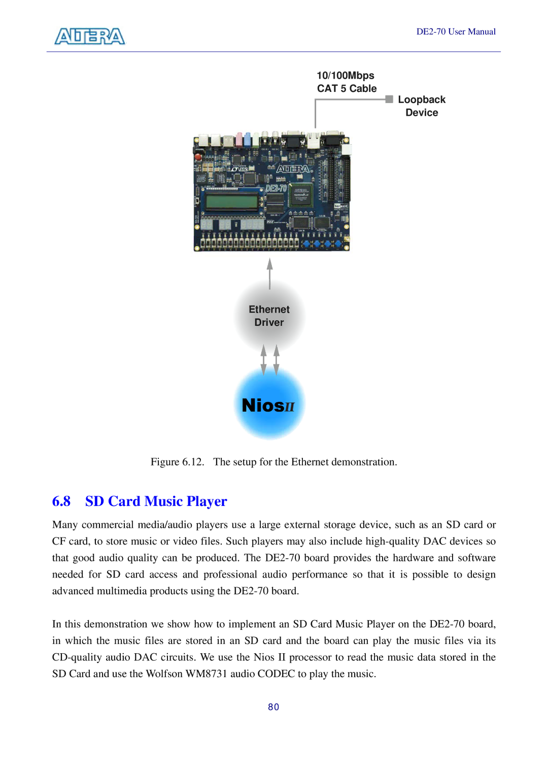
Version
Copyright 2007 Terasic Technologies
Chapter 4 DE2-70 Video Utility
Chapter 5 Using the DE2-70 Board
Altera DE2 Board
Chapter 3 DE2-70 Control Panel
Altera DE2 Board
Chapter 6 Examples of Advanced Demonstrations
Chapter 7 Appendix
DE2-70 User Manual
1.1 Package Contents
DE2-70 Package
Chapter
1.2 The DE2-70 Board Assembly
San Jose, California, 95134 USA Email university@altera.com
1.3 Getting Help
Terasic Technologies No. 356, Sec. 1, Fusing E. Rd
Altera Corporation 101 Innovation Drive
Chapter
Altera DE2-70 Board
2.1 Layout and Components
2.2 Block Diagram of the DE2-70 Board
Cyclone II 2C70 FPGA
Serial Configuration device and USB Blaster circuit
SDRAM
Pushbutton switches
Toggle switches
SSRAM
10/100 Ethernet controller
Audio CODEC
VGA output
NTSC/PAL/ SECAM TV decoder circuit
Two 40-pin expansion headers
2.3 Power-up the DE2-70 Board
Serial ports
IrDA transceiver
The LCD display shows Welcome to the Altera DE2-70
Chapter
3.1 Control Panel Setup
DE2-70 Control Panel
Figure 3.1. The DE2-70 Control Panel
3.2 Controlling the LEDs, 7-Segment Displays and LCD Display
DE2-70 User Manual
Figure 3.3. Controlling LEDs
Figure 3.4. Controlling 7-SEG display
3.3 Switches and Buttons
3.4 SDRAM/SSRAM/Flash Controller and Programmer
Figure 3.7. Accessing the SDRAM-U1
3.5 USB Monitoring
3. Press Load Memory Content to a File button
3.6 PS2 Device
3.7 SD CARD
3.8 Audio Playing and Recording
Figure 3.11. Playing audio from a selected wave file
3.9 Overall Structure of the DE2-70 Control Panel
FPGA/ SOPC
Figure 3.13. The block diagram of the DE2-70 control panel
DE2-70 User Manual
Chapter
4.1 Video Utility Setup
DE2-70 Video Utility
4.2 VGA Display
4.3 Video Capture
4.4 Overall Structure of the DE2-70 Video Utility
Figure 4.4. Video Capture Block Diagram
Chapter
Using the DE2-70 Board
5.1 Configuring the Cyclone II FPGA
FPGA
Configuring the FPGA in JTAG Mode
Configuring the EPCS16 in AS Mode
5.2 Using the LEDs and Switches
Figure 5.4. Schematic diagram of the pushbutton and toggle switches
FPGA Pin No
Figure 5.5. Schematic diagram of the LEDs
Signal Name
DE2-70 User Manual
DE2-70 User Manual
Table 5.1. Pin assignments for the toggle switches
Table 5.2. Pin assignments for the pushbutton switches
5.3 Using the 7-segment Displays
DE2-70 User Manual
5.4 Clock Circuitry
DE2-70 User Manual
Figure 5.8. Block diagram of the clock distribution
Connector
Table 5.5. Pin assignments for the clock inputs
16 DIGIT LCD
5.5 Using the LCD Module
5.6 Using the Expansion Header
1.8V 2.5V
protection registors and diodes not shown for other ports
DE2-70 User Manual
DE2-70 User Manual
DE2-70 User Manual
Table 5.8. Pin assignments for the expansion headers
5.7 Using VGA
Figure 5.13. VGA horizontal timing specification
DE2-70 User Manual
Table 5.11. ADV7123 pin assignments
5.8 Using the 24-bit Audio CODEC
5.10 PS/2 Serial Port
5.9 RS-232 Serial Port
5.11 Fast Ethernet Network Controller
DE2-70 User Manual
Figure 5.17. Fast Ethernet schematic
5.12 TV Decoder
DE2-70 User Manual
Figure 5.18. TV Decoder schematic
5.13 Implementing a TV Encoder
5.14 Using USB Host and Device
http//techtrain.microchip.com/webseminars/documents/IrDABW.pdf
5.15 Using IrDA
5.16 Using SDRAM/SRAM/Flash
SDRAM1
Figure 5.22. SDRAM schematic
DE2-70 User Manual
SDRAM0
SSRAM 512Kx36
Figure 5.23. SSRAM schematic
Figure 5.24. Flash schematic
DE2-70 User Manual
DRAM0A0
DE2-70 User Manual
DRAM0CKE
DE2-70 User Manual
DE2-70 User Manual
Table 5.19. SDRAM pin assignments
SRAM Burst Address Advance
DE2-70 User Manual
SRAM Controller Address Status
SRAM Processor Address Status
DE2-70 User Manual
Table 5.20. SSRAM pin assignments
DE2-70 User Manual
Table 5.21. Flash pin assignments
Bit stream used DE270Default.sof or DE270Default.pof
6.1 DE2-70 Factory Configuration
Installing the Demonstrations
Demonstration Setup, File Locations, and Instructions
6.2 TV Box Demonstration
Demonstration Setup, File Locations, and Instructions
Figure 6.1. Block diagram of the TV box demonstration
monitor
Bit stream used DE270TV.sof or DE270TV.pof
6.3 TV Box Picture in Picture PIP Demonstration
PiPposition
Bit stream used DE270TVPIP.sof or DE270TVPIP.pof
Demonstration Setup, File Locations, and Instructions
signal
Load the bit stream into FPGA
6.4 USB Paintbrush
Demonstration Setup, File Locations, and Instructions
Project directory DE270NIOSHOSTMOUSEVGA
Bit stream used DE270NIOSHOSTMOUSEVGA.sof
Nios II Workspace DE270NIOSHOSTMOUSEVGA\Software
6.5 USB Device
Demonstration Setup, File Locations, and Instructions
Project directory DE270NIOSDEVICELED\HW
Bit stream used DE270NIOSDEVICELED.sof
Nios II Workspace DE270NIOSDEVICELED\HW\Software
6.6 A Karaoke Machine
Figure 6.9. Block diagram of the Karaoke Machine demonstration
Bit stream used DE2-70i2sound.sof or DE2-70i2sound.pof
Demonstration Setup, File Locations, and Instructions
Clock/Data Frequency Generator
6.7 Ethernet Packet Sending/Receiving
MP3/Any Audio Output Speaker Microphone
Demonstration Setup, File Locations, and Instructions
6.8 SD Card Music Player
Figure 6.13. Block diagram of the SD music player demonstration
Demonstration Setup, File Locations, and Instructions
Project directory DE270SDCardAudioPlayer
Bit stream used DE270SDCardAudioPlayer.sof
Nios II Workspace DE270SDCardAudioPlayer\Software
6.9 Music Synthesizer Demonstration
Figure 6.17 illustrates the setup for this demonstration
Demonstration Setup, File Locations, and Instructions
Bit stream used DE270Synthesizer.sof or DE2-70Synthesizer.pof
VGALCD/CRTMonitor
DE2-70 User Manual
Line Out
Speaker
6.10 Audio Recording and Playing
Demonstration Setup, File Locations, and Instructions
SOPC
Software Project directory DE270AUDIO\software\projectaudio
Load the Software Execution File into FPGA. note *1
Chapter
Appendix
Revision History
Copyright Statement