TTCAN | User’s Manual | Revision 1.6 |
manual_about.fm
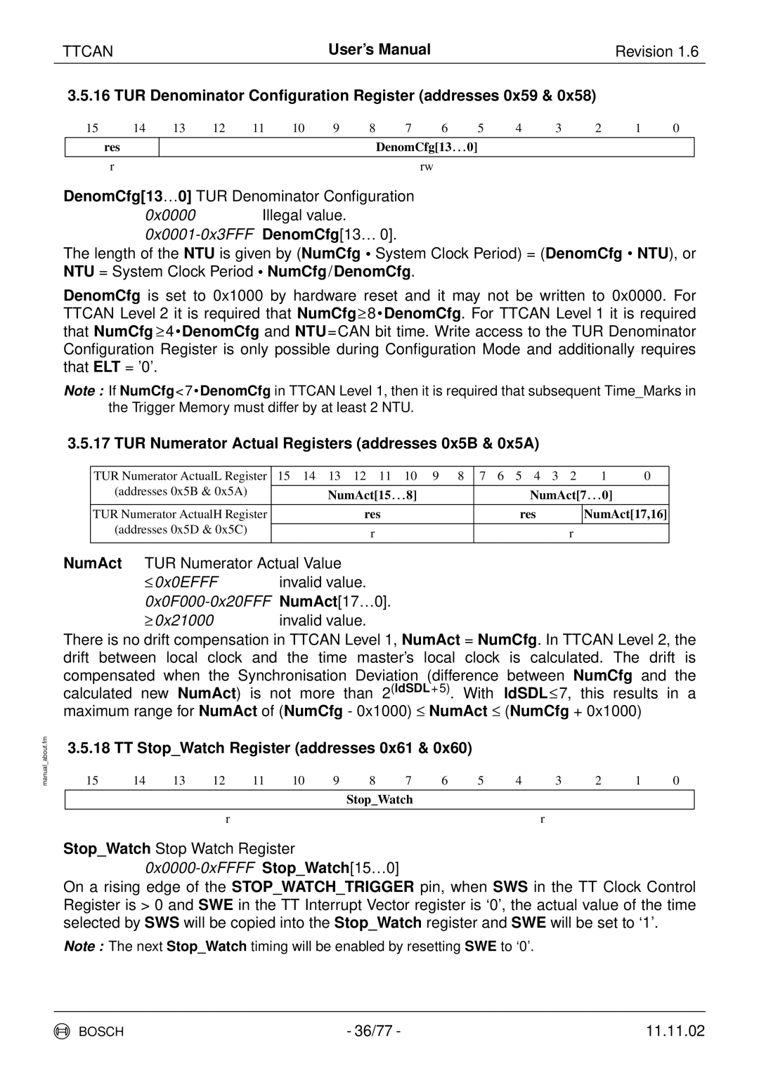
3.5.16 TUR Denominator Configuration Register (addresses 0x59 & 0x58)
15 | 14 | 13 | 12 | 11 | 10 | 9 | 8 | 7 | 6 | 5 | 4 | 3 | 2 | 1 | 0 | |
|
| res |
|
|
|
|
|
| DenomCfg[13…0] |
|
|
|
|
|
| |
|
|
|
|
|
|
|
|
|
|
|
|
|
|
|
|
|
|
| r |
|
|
|
|
|
|
| rw |
|
|
|
|
|
|
DenomCfg[13…0] TUR Denominator Configuration |
|
|
|
|
|
|
| |||||||||
|
| 0x0000 |
| Illegal value. |
|
|
|
|
|
|
|
|
| |||
|
|
|
|
|
|
|
|
|
| |||||||
The length of the NTU is given by (NumCfg • System Clock Period) = (DenomCfg • NTU), or NTU = System Clock Period • NumCfg/DenomCfg.
DenomCfg is set to 0x1000 by hardware reset and it may not be written to 0x0000. For TTCAN Level 2 it is required that NumCfg≥8•DenomCfg. For TTCAN Level 1 it is required that NumCfg ≥4•DenomCfg and NTU=CAN bit time. Write access to the TUR Denominator Configuration Register is only possible during Configuration Mode and additionally requires that ELT = ’0’.
Note : If NumCfg<7•DenomCfg in TTCAN Level 1, then it is required that subsequent Time_Marks in the Trigger Memory must differ by at least 2 NTU.
3.5.17 TUR Numerator Actual Registers (addresses 0x5B & 0x5A)
| TUR Numerator ActualL Register | 15 14 13 12 11 10 9 | 8 | 7 6 5 4 3 2 | 1 | 0 |
| (addresses 0x5B & 0x5A) |
|
|
|
| |
| NumAct[15…8] |
| NumAct[7…0] |
| ||
|
|
|
|
|
| |
| TUR Numerator ActualH Register | res |
| res | NumAct[17,16] | |
| (addresses 0x5D & 0x5C) |
|
|
|
|
|
| r |
| r |
|
| |
|
|
|
|
| ||
|
|
|
|
|
|
|
NumAct TUR Numerator Actual Value |
|
|
|
| ||
| ≤0x0EFFF | invalid value. |
|
|
|
|
|
|
|
|
|
| |
| ≥0x21000 | invalid value. |
|
|
|
|
There is no drift compensation in TTCAN Level 1, NumAct = NumCfg. In TTCAN Level 2, the drift between local clock and the time master’s local clock is calculated. The drift is
compensated when the Synchronisation Deviation (difference between NumCfg and the calculated new NumAct) is not more than 2(ldSDL+5). With ldSDL≤7, this results in a
maximum range for NumAct of (NumCfg - 0x1000) ≤ NumAct ≤ (NumCfg + 0x1000)
3.5.18 TT Stop_Watch Register (addresses 0x61 & 0x60)
15 | 14 | 13 | 12 | 11 | 10 | 9 | 8 | 7 | 6 | 5 | 4 | 3 | 2 | 1 | 0 |
|
|
|
|
|
|
| Stop_Watch |
|
|
|
|
|
|
| |
|
|
|
|
|
|
|
|
|
|
|
|
|
|
|
|
|
|
|
| r |
|
|
|
|
|
|
| r |
|
|
|
Stop_Watch Stop Watch Register
0x0000-0xFFFF Stop_Watch[15…0]
On a rising edge of the STOP_WATCH_TRIGGER pin, when SWS in the TT Clock Control Register is > 0 and SWE in the TT Interrupt Vector register is ‘0’, the actual value of the time selected by SWS will be copied into the Stop_Watch register and SWE will be set to ‘1’.
Note : The next Stop_Watch timing will be enabled by resetting SWE to ‘0’.
BOSCH | - 36/77 - | 11.11.02 |
