Cypress CY7C67200 manual Introduction, Processor Core Functional Overview, Interface Descriptions

Models: CY7C67200

1 78
Download 78 pages 5 Kb
Page 2
Image 2
Introduction

CY7C67200

Introduction

EZ-OTG™ (CY7C67200) is Cypress Semiconductor’s first USB On-The-Go (OTG) host/peripheral controller. EZ-OTG is designed to easily interface to most high-performance CPUs to add USB host functionality. EZ-OTG has its own 16-bit RISC processor to act as a coprocessor or operate in standalone mode. EZ-OTG also has a programmable IO interface block allowing a wide range of interface options.

Processor Core Functional Overview

An overview of the processor core components are presented in this section.

Processor

EZ-OTG has a general purpose 16-bit embedded RISC processor that runs at 48 MHz.

Clocking

EZ-OTG requires a 12 MHz source for clocking. Either an external crystal or TTL-level oscillator may be used. EZ-OTG has an internal PLL that produces a 48 MHz internal clock from the 12 MHz source.

Memory

EZ-OTG has a built-in 4K × 16 masked ROM and an 8K × 16 internal RAM. The masked ROM contains the EZ-OTG BIOS. The internal RAM can be used for program code or data.

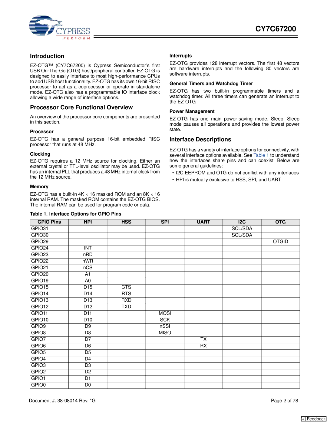
Table 1. Interface Options for GPIO Pins

Interrupts

EZ-OTG provides 128 interrupt vectors. The first 48 vectors are hardware interrupts and the following 80 vectors are software interrupts.

General Timers and Watchdog Timer

EZ-OTG has two built-in programmable timers and a watchdog timer. All three timers can generate an interrupt to the EZ-OTG.

Power Management

EZ-OTG has one main power-saving mode, Sleep. Sleep mode pauses all operations and provides the lowest power state.

Interface Descriptions

EZ-OTG has a variety of interface options for connectivity, with several interface options available. See Table 1 to understand how the interfaces share pins and can coexist. Below are some general guidelines:

I2C EEPROM and OTG do not conflict with any interfaces

HPI is mutually exclusive to HSS, SPI, and UART


GPIO Pins

HPI

HSS

SPI

UART

I2C

OTG


GPIO31


SCL/SDA


GPIO30


SCL/SDA


GPIO29


OTGID


GPIO24

INT


GPIO23

nRD


GPIO22

nWR


GPIO21

nCS


GPIO20

A1


GPIO19

A0


GPIO15

D15

CTS


GPIO14

D14

RTS


GPIO13

D13

RXD


GPIO12

D12

TXD


GPIO11

D11


MOSI


GPIO10

D10


SCK


GPIO9

D9


nSSI


GPIO8

D8


MISO


GPIO7

D7


TX


GPIO6

D6


RX


GPIO5

D5


GPIO4

D4


GPIO3

D3


GPIO2

D2


GPIO1

D1


GPIO0

D0


Document #: 38-08014 Rev. *G


Page 2 of 78

[+] Feedback

Page 2
Image 2
Cypress CY7C67200 manual Introduction, Processor Core Functional Overview, Interface Descriptions