CY7C67200
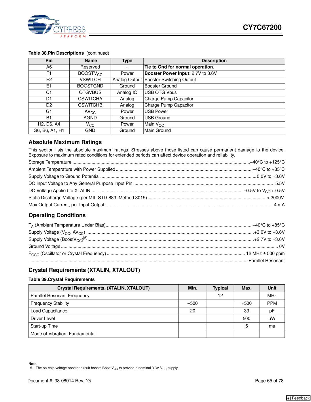
Table 38.Pin Descriptions (continued) |
|
| |
|
|
|
|
Pin | Name | Type | Description |
A6 | Reserved | – | Tie to Gnd for normal operation. |
F1 | BOOSTVCC | Power | Booster Power Input: 2.7V to 3.6V |
E2 | VSWITCH | Analog Output | Booster Switching Output |
E1 | BOOSTGND | Ground | Booster Ground |
C1 | OTGVBUS | Analog IO | USB OTG Vbus |
D1 | CSWITCHA | Analog | Charge Pump Capacitor |
D2 | CSWITCHB | Analog | Charge Pump Capacitor |
G1 | AVCC | Power | USB Power |
B1 | AGND | Ground | USB Ground |
H2, D6, A4 | VCC | Power | Main VCC |
G6, B6, A1, H1 | GND | Ground | Main Ground |
Absolute Maximum Ratings
This section lists the absolute maximum ratings. Stresses above those listed can cause permanent damage to the device. Exposure to maximum rated conditions for extended periods can affect device operation and reliability.
Storage Temperature | |
Ambient Temperature with Power Supplied | |
Supply Voltage to Ground Potential | 0.0V to +3.6V |
DC Input Voltage to Any General Purpose Input Pin | 5.5V |
DC Voltage Applied to XTALIN | |
Static Discharge Voltage (per | > 2000V |
Max Output Current, per Input Output | 4 mA |
Operating Conditions
TA (Ambient Temperature Under Bias) | |
Supply Voltage (VCC, AVCC) | +3.0V to +3.6V |
Supply Voltage (BoostV )[5] | +2.7V to +3.6V |
CC |
|
Ground Voltage | 0V |
FOSC (Oscillator or Crystal Frequency) | 12 MHz ± 500 ppm |
............................................................................................................................................................................ | Parallel Resonant |
Crystal Requirements (XTALIN, XTALOUT)
Table 39.Crystal Requirements
Crystal Requirements, (XTALIN, XTALOUT) | Min. | Typical | Max. | Unit |
Parallel Resonant Frequency |
| 12 |
| MHz |
|
|
|
|
|
Frequency Stability |
| +500 | PPM | |
|
|
|
|
|
Load Capacitance | 20 |
| 33 | pF |
|
|
|
|
|
Driver Level |
|
| 500 | µW |
|
|
|
|
|
|
| 5 | ms | |
|
|
|
|
|
Mode of Vibration: Fundamental |
|
|
|
|
|
|
|
|
|
Note
5. The
Document #: | Page 65 of 78 |
[+] Feedback