CY7C67200
Register Summary
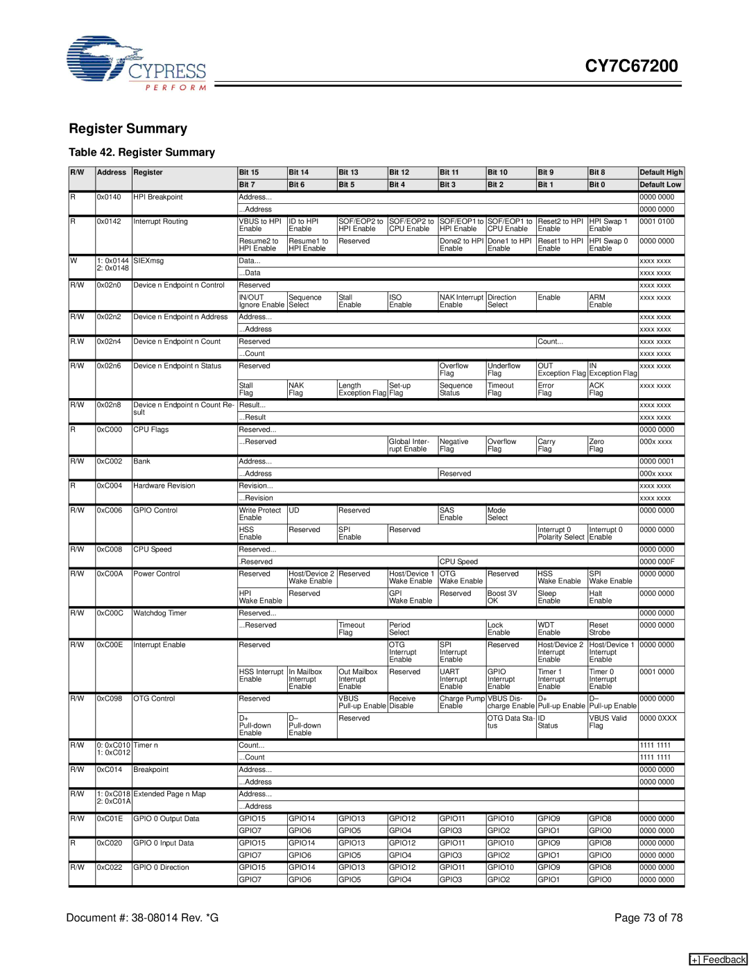
Table 42. Register Summary
R/W | Address | Register | Bit 15 | Bit 14 | Bit 13 | Bit 12 | Bit 11 | Bit 10 | Bit 9 | Bit 8 | Default High |
|
|
| Bit 7 | Bit 6 | Bit 5 | Bit 4 | Bit 3 | Bit 2 | Bit 1 | Bit 0 | Default Low |
R | 0x0140 | HPI Breakpoint | Address... |
|
|
|
|
|
|
| 0000 0000 |
|
|
| ...Address |
|
|
|
|
|
|
| 0000 0000 |
R | 0x0142 | Interrupt Routing | VBUS to HPI | ID to HPI | SOF/EOP2 to | SOF/EOP2 to | SOF/EOP1 to | SOF/EOP1 to | Reset2 to HPI | HPI Swap 1 | 0001 0100 |
|
|
| Enable | Enable | HPI Enable | CPU Enable | HPI Enable | CPU Enable | Enable | Enable |
|
|
|
| Resume2 to | Resume1 to | Reserved |
| Done2 to HPI | Done1 to HPI | Reset1 to HPI | HPI Swap 0 | 0000 0000 |
|
|
| HPI Enable | HPI Enable |
|
| Enable | Enable | Enable | Enable |
|
W | 1: 0x0144 | SIEXmsg | Data... |
|
|
|
|
|
|
| xxxx xxxx |
| 2: 0x0148 |
|
|
|
|
|
|
|
|
|
|
|
| ...Data |
|
|
|
|
|
|
| xxxx xxxx | |
|
|
|
|
|
|
|
|
|
| ||
R/W | 0x02n0 | Device n Endpoint n Control | Reserved |
|
|
|
|
|
|
| xxxx xxxx |
|
|
| IN/OUT | Sequence | Stall | ISO | NAK Interrupt | Direction | Enable | ARM | xxxx xxxx |
|
|
| Ignore Enable | Select | Enable | Enable | Enable | Select |
| Enable |
|
R/W | 0x02n2 | Device n Endpoint n Address | Address... |
|
|
|
|
|
|
| xxxx xxxx |
|
|
| ...Address |
|
|
|
|
|
|
| xxxx xxxx |
R.W | 0x02n4 | Device n Endpoint n Count | Reserved |
|
|
|
|
| Count... |
| xxxx xxxx |
|
|
| ...Count |
|
|
|
|
|
|
| xxxx xxxx |
R/W | 0x02n6 | Device n Endpoint n Status | Reserved |
|
|
| Overflow | Underflow | OUT | IN | xxxx xxxx |
|
|
|
|
|
|
| Flag | Flag | Exception Flag | Exception Flag |
|
|
|
| Stall | NAK | Length | Sequence | Timeout | Error | ACK | xxxx xxxx | |
|
|
| Flag | Flag | Exception Flag | Flag | Status | Flag | Flag | Flag |
|
R/W | 0x02n8 | Device n Endpoint n Count Re- | Result... |
|
|
|
|
|
|
| xxxx xxxx |
|
| sult |
|
|
|
|
|
|
|
|
|
|
| ...Result |
|
|
|
|
|
|
| xxxx xxxx | |
|
|
|
|
|
|
|
|
|
| ||
R | 0xC000 | CPU Flags | Reserved... |
|
|
|
|
|
|
| 0000 0000 |
|
|
| ...Reserved |
|
| Global Inter- | Negative | Overflow | Carry | Zero | 000x xxxx |
|
|
|
|
|
| rupt Enable | Flag | Flag | Flag | Flag |
|
R/W | 0xC002 | Bank | Address... |
|
|
|
|
|
|
| 0000 0001 |
|
|
| ...Address |
|
|
| Reserved |
|
|
| 000x xxxx |
R | 0xC004 | Hardware Revision | Revision... |
|
|
|
|
|
|
| xxxx xxxx |
|
|
| ...Revision |
|
|
|
|
|
|
| xxxx xxxx |
R/W | 0xC006 | GPIO Control | Write Protect | UD | Reserved |
| SAS | Mode |
|
| 0000 0000 |
|
|
| Enable |
|
|
| Enable | Select |
|
|
|
|
|
| HSS | Reserved | SPI | Reserved |
|
| Interrupt 0 | Interrupt 0 | 0000 0000 |
|
|
| Enable |
| Enable |
|
|
| Polarity Select | Enable |
|
R/W | 0xC008 | CPU Speed | Reserved... |
|
|
|
|
|
|
| 0000 0000 |
|
|
| .Reserved |
|
|
| CPU Speed |
|
|
| 0000 000F |
R/W | 0xC00A | Power Control | Reserved | Host/Device 2 | Reserved | Host/Device 1 | OTG | Reserved | HSS | SPI | 0000 0000 |
|
|
|
| Wake Enable |
| Wake Enable | Wake Enable |
| Wake Enable | Wake Enable |
|
|
|
| HPI | Reserved |
| GPI | Reserved | Boost 3V | Sleep | Halt | 0000 0000 |
|
|
| Wake Enable |
|
| Wake Enable |
| OK | Enable | Enable |
|
R/W | 0xC00C | Watchdog Timer | Reserved... |
|
|
|
|
|
|
| 0000 0000 |
|
|
| ...Reserved |
| Timeout | Period |
| Lock | WDT | Reset | 0000 0000 |
|
|
|
|
| Flag | Select |
| Enable | Enable | Strobe |
|
R/W | 0xC00E | Interrupt Enable | Reserved |
|
| OTG | SPI | Reserved | Host/Device 2 | Host/Device 1 | 0000 0000 |
|
|
|
|
|
| Interrupt | Interrupt |
| Interrupt | Interrupt |
|
|
|
|
|
|
| Enable | Enable |
| Enable | Enable |
|
|
|
| HSS Interrupt | In Mailbox | Out Mailbox | Reserved | UART | GPIO | Timer 1 | Timer 0 | 0001 0000 |
|
|
| Enable | Interrupt | Interrupt |
| Interrupt | Interrupt | Interrupt | Interrupt |
|
|
|
|
| Enable | Enable |
| Enable | Enable | Enable | Enable |
|
R/W | 0xC098 | OTG Control | Reserved |
| VBUS | Receive | Charge Pump | VBUS Dis- | D+ | D– | 0000 0000 |
|
|
|
|
| Disable | Enable | charge Enable |
| |||
|
|
| D+ | D– | Reserved |
|
| OTG Data Sta- | ID | VBUS Valid | 0000 0XXX |
|
|
|
|
|
| tus | Status | Flag |
| ||
|
|
| Enable | Enable |
|
|
|
|
|
|
|
R/W | 0: 0xC010 | Timer n | Count... |
|
|
|
|
|
|
| 1111 1111 |
| 1: 0xC012 |
|
|
|
|
|
|
|
|
|
|
|
| ...Count |
|
|
|
|
|
|
| 1111 1111 | |
|
|
|
|
|
|
|
|
|
| ||
R/W | 0xC014 | Breakpoint | Address... |
|
|
|
|
|
|
| 0000 0000 |
|
|
| ...Address |
|
|
|
|
|
|
| 0000 0000 |
R/W | 1: 0xC018 | Extended Page n Map | Address... |
|
|
|
|
|
|
|
|
| 2: 0xC01A |
|
|
|
|
|
|
|
|
|
|
|
| ...Address |
|
|
|
|
|
|
|
| |
|
|
|
|
|
|
|
|
|
|
| |
R/W | 0xC01E | GPIO 0 Output Data | GPIO15 | GPIO14 | GPIO13 | GPIO12 | GPIO11 | GPIO10 | GPIO9 | GPIO8 | 0000 0000 |
|
|
| GPIO7 | GPIO6 | GPIO5 | GPIO4 | GPIO3 | GPIO2 | GPIO1 | GPIO0 | 0000 0000 |
R | 0xC020 | GPIO 0 Input Data | GPIO15 | GPIO14 | GPIO13 | GPIO12 | GPIO11 | GPIO10 | GPIO9 | GPIO8 | 0000 0000 |
|
|
| GPIO7 | GPIO6 | GPIO5 | GPIO4 | GPIO3 | GPIO2 | GPIO1 | GPIO0 | 0000 0000 |
R/W | 0xC022 | GPIO 0 Direction | GPIO15 | GPIO14 | GPIO13 | GPIO12 | GPIO11 | GPIO10 | GPIO9 | GPIO8 | 0000 0000 |
|
|
| GPIO7 | GPIO6 | GPIO5 | GPIO4 | GPIO3 | GPIO2 | GPIO1 | GPIO0 | 0000 0000 |
Document #: | Page 73 of 78 |
[+] Feedback