CY7C67200
External (Remote) Wakeup Source
There are several possible events available to wake
Upon wakeup, code begins executing within 200 ms, the time it takes the PLL to stabilize.
Table 15.wakeup Sources[3, 4]
Wakeup Source (if enabled) | Event |
USB Resume | D+/D– Signaling |
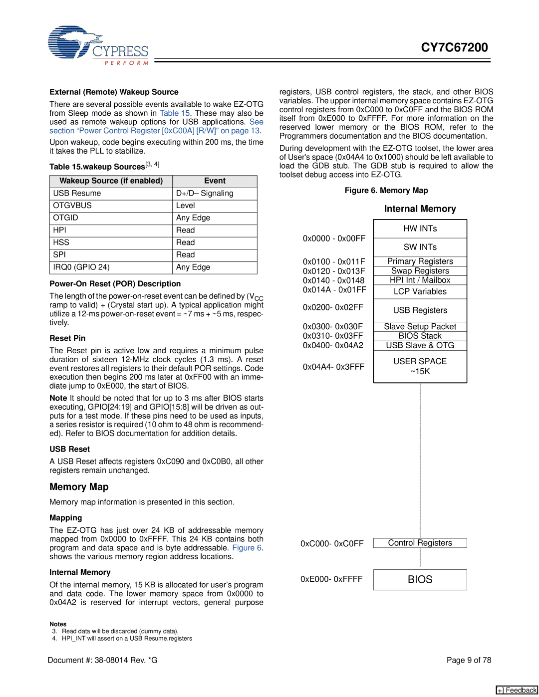
registers, USB control registers, the stack, and other BIOS variables. The upper internal memory space contains
During development with the
Figure 6. Memory Map
OTGVBUS | Level |
OTGID | Any Edge |
|
|
HPI | Read |
|
|
HSS | Read |
|
|
SPI | Read |
|
|
IRQ0 (GPIO 24) | Any Edge |
Power-On Reset (POR) Description
The length of the
Reset Pin
The Reset pin is active low and requires a minimum pulse duration of sixteen
Note It should be noted that for up to 3 ms after BIOS starts executing, GPIO[24:19] and GPIO[15:8] will be driven as out- puts for a test mode. If these pins need to be used as inputs, a series resistor is required (10 ohm to 48 ohm is recommend- ed). Refer to BIOS documentation for addition details.
USB Reset
A USB Reset affects registers 0xC090 and 0xC0B0, all other registers remain unchanged.
Memory Map
Memory map information is presented in this section.
Mapping
0x0000 - 0x00FF
0x0100 - 0x011F
0x0120 - 0x013F
0x0140 - 0x0148 0x014A - 0x01FF
0x0200- 0x02FF
0x0300- 0x030F
0x0310- 0x03FF
0x0400- 0x04A2
0x04A4- 0x3FFF
Internal Memory
HW INTs
SW INTs
Primary Registers
Swap Registers
HPI Int / Mailbox
LCP Variables
USB Registers
Slave Setup Packet
BIOS Stack
USB Slave & OTG
USER SPACE
~15K
The
Internal Memory
Of the internal memory, 15 KB is allocated for user’s program and data code. The lower memory space from 0x0000 to 0x04A2 is reserved for interrupt vectors, general purpose
Notes
3.Read data will be discarded (dummy data).
4.HPI_INT will assert on a USB Resume.registers
0xC000- 0xC0FF | Control Registers |
0xE000- 0xFFFF | BIOS |
Document #: | Page 9 of 78 |
[+] Feedback