CY7C67200
CRC Enable (Bit 13)
The CRC Enable bit enables or disables the CRC operation.
1:Enables CRC operation
0:Disables CRC operation
CRC Clear (Bit 12)
The CRC Clear bit will clear the CRC with a load of all ones. This bit is self clearing and always reads ‘0’.
1:Clear CRC with all ones
0:No Function
Receive CRC (Bit 11)
The Receive CRC bit determines whether the receive bit stream or the transmit bit stream is used for the CRC data input in full duplex mode. This bit is a don’t care in
1:Assigns the receive bit stream
0:Assigns the transmit bit stream
SPI CRC Value Register [0xC0D4] [R/W]
One in CRC (Bit 10)
The One in CRC bit is a
1:CRC value is not all zeros
0:CRC value is all zeros
Zero in CRC (Bit 9)
The Zero in CRC bit is a
1:CRC value is not all ones
0:CRC value is all ones
Reserved
All reserved bits must be written as ‘0’.
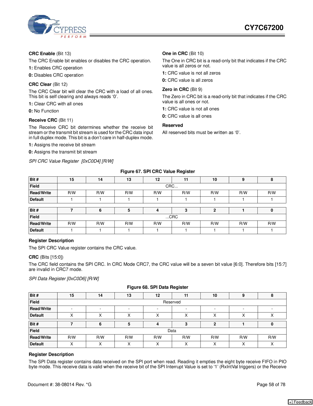
Figure 67. SPI CRC Value Register
Bit # | 15 | 14 | 13 | 12 |
| 11 | 10 | 9 | 8 |
Field |
|
|
|
| CRC... |
|
|
| |
Read/Write | R/W | R/W | R/W | R/W |
| R/W | R/W | R/W | R/W |
Default | 1 | 1 | 1 | 1 |
| 1 | 1 | 1 | 1 |
|
|
|
|
|
|
|
|
|
|
Bit # | 7 | 6 | 5 | 4 |
| 3 | 2 | 1 | 0 |
Field |
|
|
|
| ...CRC |
|
|
| |
Read/Write | R/W | R/W | R/W | R/W |
| R/W | R/W | R/W | R/W |
Default | 1 | 1 | 1 | 1 |
| 1 | 1 | 1 | 1 |
|
|
|
|
|
|
|
|
|
|
Register Description
The SPI CRC Value register contains the CRC value.
CRC (Bits [15:0])
The CRC field contains the SPI CRC. In CRC Mode CRC7, the CRC value will be a seven bit value [6:0]. Therefore bits [15:7] are invalid in CRC7 mode.
SPI Data Register [0xC0D6] [R/W]
Figure 68. SPI Data Register
Bit # | 15 | 14 | 13 | 12 |
| 11 | 10 | 9 | 8 |
Field |
|
|
|
| Reserved |
|
|
| |
Read/Write | - | - | - | - |
| - | - | - | - |
Default | X | X | X | X |
| X | X | X | X |
|
|
|
|
|
|
|
|
|
|
Bit # | 7 | 6 | 5 | 4 |
| 3 | 2 | 1 | 0 |
Field |
|
|
|
| Data |
|
|
| |
Read/Write | R/W | R/W | R/W | R/W |
| R/W | R/W | R/W | R/W |
Default | X | X | X | X |
| X | X | X | X |
|
|
|
|
|
|
|
|
|
|
Register Description
The SPI Data register contains data received on the SPI port when read. Reading it empties the eight byte receive FIFO in PIO byte mode. This receive data is valid when the receive bit of the SPI Interrupt Value is set to ‘1’ (RxIntVal triggers) or the Receive
Document #: | Page 58 of 78 |
[+] Feedback