CY7C67200
Host Port Interface (HPI)
Note It should be noted that for up to 3 ms after BIOS starts executing, GPIO[24:19] and GPIO[15:8] will be driven as outputs for a test mode. If these pins need to be used as inputs, a series resistor is required (10 ohm to 48 ohm is recom- mended). Refer to BIOS documentation for addition details. See section “Reset Pin” on page 9.
HPI Features
•
•16 MB/s throughput
•
•Direct memory access (DMA) to internal memory
•Bidirectional Mailbox register
•Byte Swapping
•Complete access to internal memory
•Complete control of SIEs through HPI
•Dedicated HPI Status register
Table 9. HPI Interface Pins [1, 2] | (continued) | |
Pin Name |
| Pin Number |
D7 |
| B5 |
|
|
|
D6 |
| B4 |
D5 |
| C4 |
|
|
|
D4 |
| B3 |
|
|
|
D3 |
| A3 |
|
|
|
D2 |
| C3 |
|
|
|
D1 |
| A2 |
D0 |
| B2 |
|
|
|
The two HPI address pins are used to address one of four possible HPI port registers as shown in Table 10 below.
Table 10.HPI Addressing
HPI A[1:0] | A1 | A0 |
HPI Data | 0 | 0 |
HPI Mailbox | 0 | 1 |
HPI Address | 1 | 0 |
HPI Status | 1 | 1 |
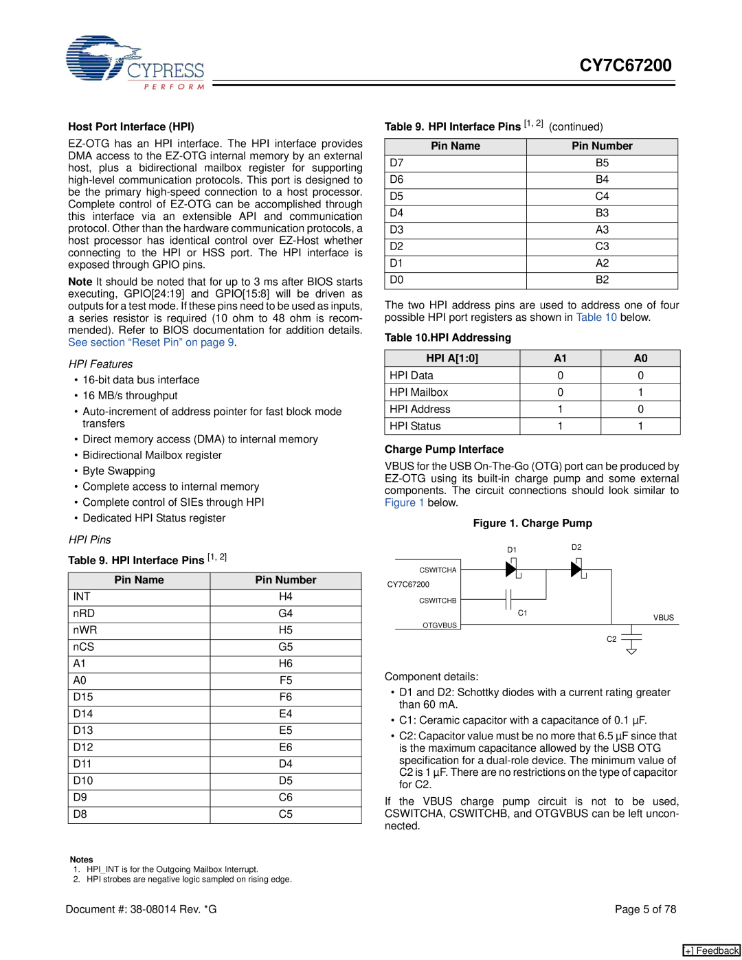
Charge Pump Interface
VBUS for the USB
Figure 1. Charge Pump
HPI Pins
Table 9. HPI Interface Pins [1, 2]
Pin Name | Pin Number |
INT | H4 |
|
|
nRD | G4 |
|
|
nWR | H5 |
|
|
nCS | G5 |
|
|
A1 | H6 |
CSWITCHA
CY7C67200
CSWITCHB
OTGVBUS
D1D2
C1 | VBUS |
| |
| C2 |
A0 | F5 |
D15 | F6 |
|
|
D14 | E4 |
|
|
D13 | E5 |
|
|
D12 | E6 |
|
|
D11 | D4 |
|
|
D10 | D5 |
|
|
D9 | C6 |
|
|
D8 | C5 |
Notes
1.HPI_INT is for the Outgoing Mailbox Interrupt.
2.HPI strobes are negative logic sampled on rising edge.
Component details:
•D1 and D2: Schottky diodes with a current rating greater than 60 mA.
•C1: Ceramic capacitor with a capacitance of 0.1 µF.
•C2: Capacitor value must be no more that 6.5 µF since that is the maximum capacitance allowed by the USB OTG specification for a
If the VBUS charge pump circuit is not to be used, CSWITCHA, CSWITCHB, and OTGVBUS can be left uncon- nected.
Document #: | Page 5 of 78 |
[+] Feedback