CY7C67200
VBUS Valid Flag (Bit 0)
The VBUS Valid Flag bit indicates whether OTG VBus is greater than 4.4V. After turning on VBUS, firmware should wait at least 10 µs before this reading this bit.
GPIO Registers
1:OTG VBus is greater then 4.4V
0:OTG VBus is less then 4.4V
Reserved
All reserved bits must be written as ‘0’.
There are seven registers dedicated for GPIO operations. These seven registers are covered in this section and summarized in Table 29.
Table 29.GPIO Registers
| Register Name |
|
|
|
| Address |
|
| R/W |
| ||||
GPIO Control Register |
|
|
|
|
| 0xC006 |
|
| R/W |
| ||||
|
|
|
|
|
|
|
|
|
|
|
|
|
|
|
GPIO0 Output Data Register |
|
|
|
|
| 0xC01E |
|
| R/W |
| ||||
|
|
|
|
|
|
|
|
|
|
|
|
|
|
|
GPIO0 Input Data Register |
|
|
|
|
| 0xC020 |
|
|
| R |
| |||
|
|
|
|
|
|
|
|
|
|
|
|
|
|
|
GPIO0 Direction Register |
|
|
|
|
| 0xC022 |
|
| R/W |
| ||||
|
|
|
|
|
|
|
|
|
|
|
|
|
|
|
GPIO1 Output Data Register |
|
|
|
|
| 0xC024 |
|
| R/W |
| ||||
|
|
|
|
|
|
|
|
|
|
|
|
|
|
|
GPIO1 Input Data Register |
|
|
|
|
| 0xC026 |
|
|
| R |
| |||
|
|
|
|
|
|
|
|
|
|
|
|
|
|
|
GPIO1 Direction Register |
|
|
|
|
| 0xC028 |
|
| R/W |
| ||||
|
|
|
|
|
|
|
|
|
|
|
|
|
| |
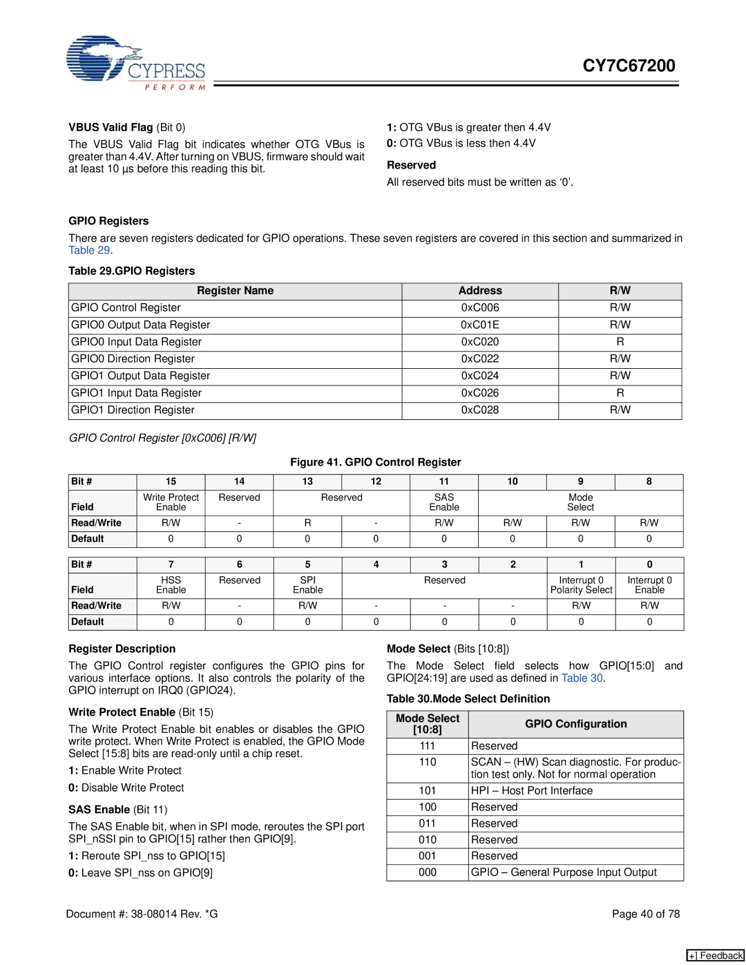
GPIO Control Register [0xC006] [R/W] |
|
|
|
|
|
|
|
|
|
|
| |||
|
|
|
| Figure 41. GPIO Control Register |
|
|
|
|
| |||||
|
|
|
|
|
|
|
|
|
|
|
|
|
| |
Bit # | 15 |
| 14 | 13 |
| 12 |
| 11 |
| 10 | 9 | 8 |
| |
Field | Write Protect |
| Reserved | Reserved |
|
| SAS |
|
|
| Mode |
|
| |
Enable |
|
|
|
|
|
| Enable |
|
|
| Select |
|
| |
Read/Write | R/W |
| - | R |
| - |
| R/W |
| R/W |
| R/W | R/W |
|
Default | 0 |
| 0 | 0 |
| 0 |
| 0 |
| 0 | 0 | 0 |
| |
|
|
|
|
|
|
|
|
|
|
|
|
|
|
|
Bit # | 7 |
| 6 | 5 |
| 4 |
| 3 |
| 2 | 1 | 0 |
| |
Field | HSS |
| Reserved | SPI |
|
|
| Reserved |
|
| Interrupt 0 | Interrupt 0 |
| |
Enable |
|
| Enable |
|
|
|
|
|
| Polarity Select | Enable |
| ||
Read/Write | R/W |
| - | R/W |
| - |
| - |
| - |
| R/W | R/W |
|
Default | 0 |
| 0 | 0 |
| 0 |
| 0 |
| 0 | 0 | 0 |
| |
|
|
|
|
|
|
|
|
|
|
|
|
|
|
|
Register Description
The GPIO Control register configures the GPIO pins for various interface options. It also controls the polarity of the GPIO interrupt on IRQ0 (GPIO24).
Write Protect Enable (Bit 15)
The Write Protect Enable bit enables or disables the GPIO write protect. When Write Protect is enabled, the GPIO Mode Select [15:8] bits are
1:Enable Write Protect
0:Disable Write Protect
SAS Enable (Bit 11)
The SAS Enable bit, when in SPI mode, reroutes the SPI port SPI_nSSI pin to GPIO[15] rather then GPIO[9].
1:Reroute SPI_nss to GPIO[15]
0:Leave SPI_nss on GPIO[9]
Mode Select (Bits [10:8])
The Mode Select field selects how GPIO[15:0] and GPIO[24:19] are used as defined in Table 30.
Table 30.Mode Select Definition
Mode Select | GPIO Configuration | |
[10:8] | ||
| ||
111 | Reserved |
110SCAN – (HW) Scan diagnostic. For produc- tion test only. Not for normal operation
101HPI – Host Port Interface
100Reserved
011Reserved
010Reserved
001Reserved
000GPIO – General Purpose Input Output
Document #: | Page 40 of 78 |
[+] Feedback