CY7C67200
UART Features
•Supports baud rates of 900 to 115.2K
•
UART Pins
Table 5. UART Interface Pins
Pin Name | Pin Number |
TX | B5 |
|
|
RX | B4 |
|
|
I2C EEPROM Interface
I2C EEPROM Features
•Supports EEPROMs up to 64 KB (512K bit)
•
I2C EEPROM Pins
Table 6. I2C EEPROM Interface Pins
Pin Name |
| Pin Number |
| SMALL | EEPROM |
|
|
|
SCK |
| H3 |
|
|
|
SDA |
| F3 |
|
|
|
| LARGE | EEPROM |
|
|
|
SCK |
| F3 |
|
|
|
SDA |
| H3 |
|
|
|
Serial Peripheral Interface
SPI Features
•Master or slave mode operation
•DMA block transfer and PIO byte transfer modes
•Full duplex or half duplex data communication
•
•Selectable master SPI clock rates from 250 kHz to 12 MHz
•Selectable master SPI clock phase and polarity
•Slave SPI signaling synchronization and filtering
•Slave SPI clock rates up to 2 MHz
•Maskable interrupts for block and byte transfer modes
•Individual bit transfer for
•Programmable delay timing for the active/inactive master SPI clock
•Auto or manual control for master mode slave select signal
•Complete access to internal memory
SPI Pins
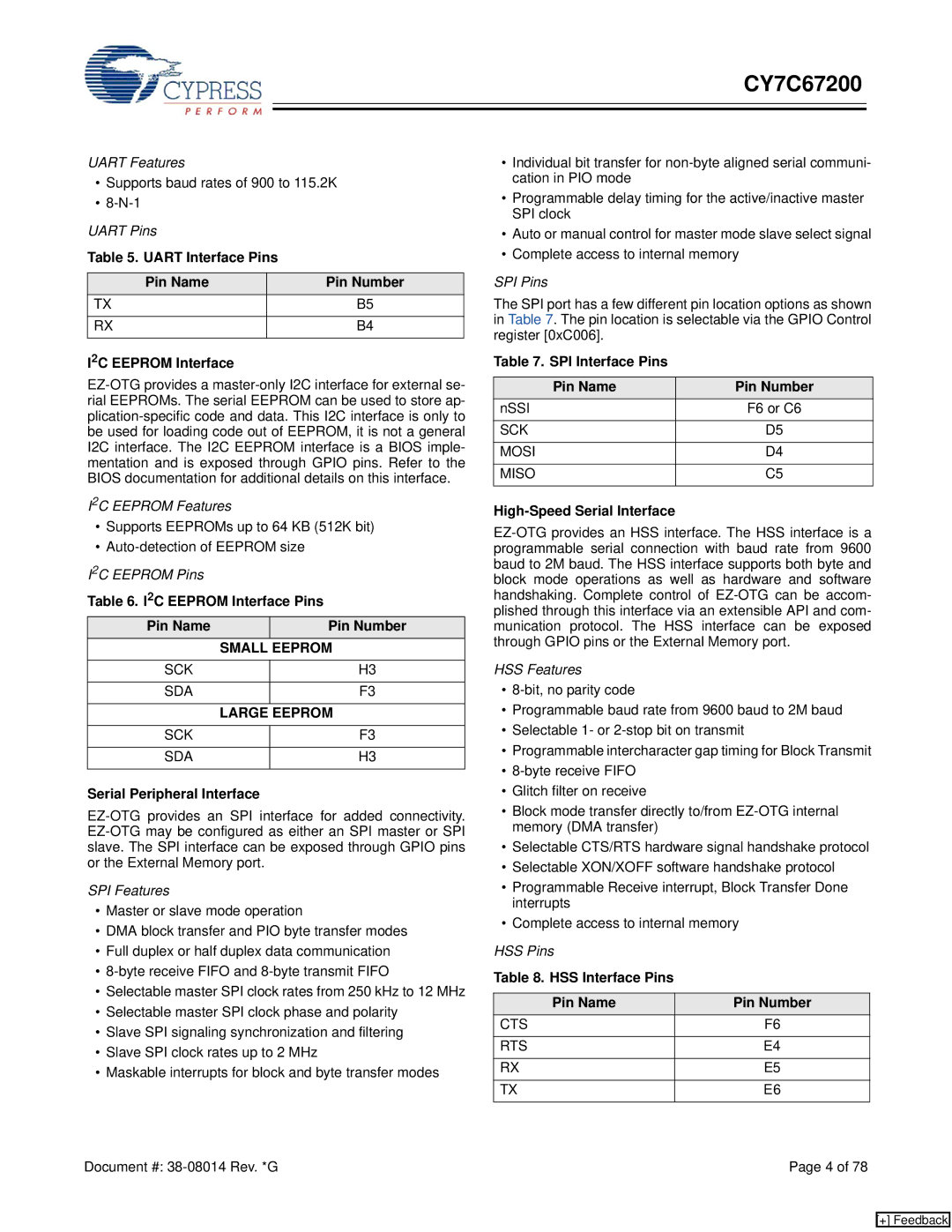
The SPI port has a few different pin location options as shown in Table 7. The pin location is selectable via the GPIO Control register [0xC006].
Table 7. SPI Interface Pins
Pin Name | Pin Number |
nSSI | F6 or C6 |
|
|
SCK | D5 |
|
|
MOSI | D4 |
|
|
MISO | C5 |
|
|
High-Speed Serial Interface
HSS Features
•
•Programmable baud rate from 9600 baud to 2M baud
•Selectable 1- or
•Programmable intercharacter gap timing for Block Transmit
•
•Glitch filter on receive
•Block mode transfer directly to/from
•Selectable CTS/RTS hardware signal handshake protocol
•Selectable XON/XOFF software handshake protocol
•Programmable Receive interrupt, Block Transfer Done interrupts
•Complete access to internal memory
HSS Pins
Table 8. HSS Interface Pins
Pin Name | Pin Number |
CTS | F6 |
|
|
RTS | E4 |
|
|
RX | E5 |
|
|
TX | E6 |
|
|
Document #: | Page 4 of 78 |
[+] Feedback
