
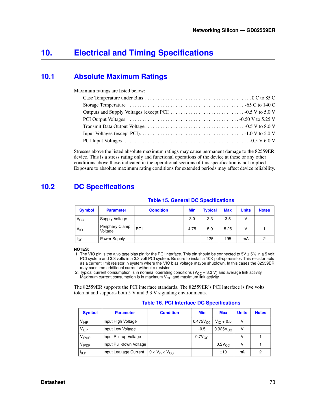
GD82559ER specifications
The Intel GD82559ER is a highly regarded network interface controller (NIC) designed for use in various computing environments, primarily for stable connectivity in both desktop and server applications. Released as part of the 82559 family of Ethernet controllers, the GD82559ER features advanced technologies that enhance performance, reliability, and manageability.One of the standout features of the 82559ER is its ability to support both 10/100 Mbps Ethernet. This dual capability allows the controller to operate in a wide range of network settings, making it adaptable to legacy systems while also providing support for modern Ethernet standards. This versatility is crucial for organizations looking to maintain operational effectiveness without the need for immediate upgrades to their existing infrastructure.
The GD82559ER employs a PCI interface, which allows it to connect with various devices and motherboards easily, making it a go-to choice for manufacturers aiming for integration in their systems. It also includes features like Auto-Negotiation, enabling the NIC to automatically detect and select the appropriate speed and duplex mode for optimal performance. This capability is essential in dynamic networking environments, where devices from various generations coexist.
Power management is another critical aspect of the GD82559ER. The controller supports advanced power-saving features like PCI Power Management, reducing energy consumption during low-usage periods. This not only contributes to lower operational costs but also aligns with modern eco-friendly initiatives in technology.
Additionally, the GD82559ER comes equipped with advanced diagnostics and monitoring capabilities. This enhances the network's manageability by allowing administrators to track performance metrics and diagnose issues effectively. Through its onboard diagnostics, the controller aids in ensuring a stable network connection, allowing for timely interventions when issues arise.
The controller is also designed with a robust architecture that supports various operating systems, facilitating a broad implementation across different platforms. As a result, the GD82559ER has become a reliable option for system builders and enterprises focused on building dependable networking solutions.
Overall, the Intel GD82559ER is a versatile, high-performance network interface controller that continues to serve as a foundational component for computer systems that require efficient, reliable networking capabilities. Its combination of technologies and features makes it a popular choice in diverse computing environments.