MCS-80/85 specifications
The Intel MCS-80/85 family, introduced in the late 1970s, is a seminal collection of microprocessors that played a pivotal role in the early days of computing. The MCS-80 series, initially targeting embedded systems and control applications, gained remarkable attention due to its innovative architecture and flexible programming capabilities.The MCS-80 family is anchored by the 8080 microprocessor, which was one of the first fully integrated 8-bit microprocessors. Released in 1974, the 8080 operated at clock speeds ranging from 2 MHz to 3 MHz and featured a 16-bit address bus capable of addressing up to 64KB of memory. The processor’s instruction set included around 78 instructions, providing extensive capabilities for data manipulation, logic operations, and branching.
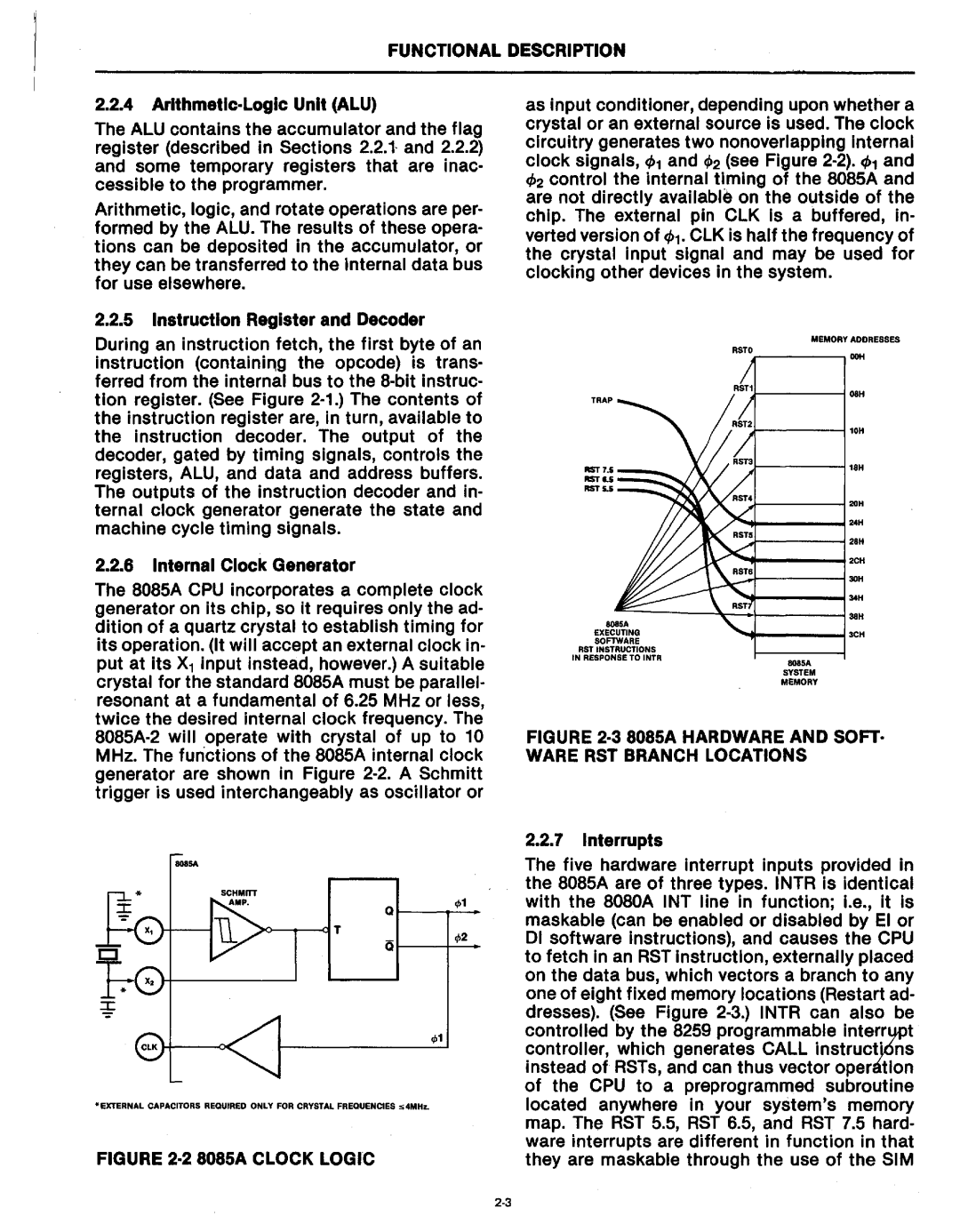
Complementing the 8080 was a suite of support chips, forming the MCS-80 platform. The most notable among them was the 8155, which integrated a static RAM, I/O ports, and a timer, tailored for ease of designing systems around the 8080. Other support chips included the 8085, which provided improvements with an integrated clock generator, making it compatible with more modern designs and applications.
The MCS-85 series, on the other hand, revolves around the 8085 microprocessor, which provided a more advanced architecture. The 8085 operated at clock speeds of up to 6 MHz and came with a 16-bit address bus, similar to its predecessor. However, it introduced more sophisticated features, including an enhanced instruction set and support for interrupt-driven programming. These enhancements made the 8085 especially appealing to developers working in real-time processing environments.
The MCS-80/85 family utilized NMOS technology, known for its lower power consumption and higher performance compared to previous technologies like TTL. The family’s architecture allowed for easy interfacing with a variety of peripherals, making it a favorite for educational institutions and hobbyists embarking on computer engineering projects.
With its robustness, versatility, and affordability, the Intel MCS-80/85 microprocessors laid the groundwork for many subsequent microcomputer systems and applications. The legacy of this powerful family continues to influence modern microprocessor design, emphasizing the importance of reliable architecture in a rapidly evolving technology landscape.