Page
Inter
INTEl Corporation
Table of Contents
Page
Introduction
Page
Chapter Part 1 Introduction to Functions of a Computer
Instruction Register and Decoder
Program Counter Jumps, Subroutines and the Stack
Address Registers
Control Circuitry
Arithmetic/Logic Unit ALU
Timing
Memory Read
Instruction Fetch
Memory Write
Wait memory synchronization
Module
Evolution
MCS·SS Microcomputer System
Introduction to MCS-85
Software Compatibility
8155 =CE, 8156 =CE
MCS·S5 Special Peripheral Components
·1. MCS·SS Basic System
MEMil. lOR
Interfacing to MCS·80/8S Programmable Peripheral Components
Programmable Peripherals
Demultiplexing the BUS
Interfacing to Standard Memory
System Performance
Instruction CYCLE/ACCESS Time
Distributed Processing
Conclusions THROUGHPUT/COST
Page
Functional Description
Page
Whatsin the 808SA
·1 808SA CPU Functional Block Diagram
122H
Hexadecimalbinary A7H
Hexidecimal Binary AEH
·28085A Clock Logic
·38085A Hardware and SOFT· Ware RST Branch Locations
·5RIM Read Interrupt Mask
·4INTERRUPT Masks SET Using SIM Instruction
Name Priority
When Inter· Rupt occurs
Type
Branched to
·8BASIC CPU Functions
HOW the MCS·85SYSTEM Works
·9 CPU Timing for Store Accumulator Direct STA Instruction
Functional Description
·12808SA Machine State Chart
·13OPCODE Fetch Machine Cycle of DCX Instruction
Lililili
Memory Write MW
Jl..Jl..Jl..J LIl..Jl..J ~
U- U-U
V V U
Lr \F LrLrU-U-U-U- U
~--r
\J li\ Lr V V- U V u u u U
·21 Hold VS Interrupt NON Halt
RST 5.5 Mask
Resets Sets
RST 6~5 Mask
RST 7.5 Mask
7J==- 10ms.c
= ~
ALE
Signals Function
AS-AI5 101M =x---C
Conclusion
Page
System Operating
Page
LOA
Mvim
STA
Lhld
Address Assignment
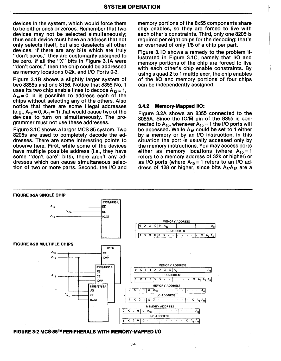
System Operation
To , , I X X X
Memory·Mapped
·-·-1
Dynamic RAM Interface
Interfacing to MCS·80 Peripherals
Interfacing to Standard BUS Memories
·3 MCS·80 Peripherals with 110 Mapped
Parts Functions
Minimum MCS-85 System
T1t
Scale =11
System Operation
·8 Expanded System
Parts Function
System Operation Expanded MCS·85 System
ROM/EPROM
CPU
Page
Functional Description
Page
Chapter 8080 Central Processor Unit
Registers
Data Bus Buffer
Arithmetic and Logic Unit ALU
Instruction Register and Control
Machine Cycle Identification
State Transition Sequence
Status Bit Definitions
$ no
Irr\
RL- rL- rL.-h rL-h -h rL-rL- r-L
State Associated Activities
LnLn
IrL
Hold Sequences
~ ~ ~~ w---t. ~~u----t
Wl ~ ~
Page
Page
Page
Page
Condition
Iiii
Instruction Set
Page
H,SP
H,L
000 B
011 E 100 H
Instruction and Data Formats
Label
Data Word
\JNN
Condition Flags
Addressing Modes
Instruction SET Encyclopedia
O o 1 1 o
Instruction SET
P,CY,AC
Xchg
ADD M
R CY
~-1 ~-·
8085, 5
P,AC
«H L
00 0 S S S
DAA
\ r
Address,jng
Cleared
RLC
ORA M
1 1 1 1
CMA
CMC
Condition
«SP
Cycles 2/5 8085,315 States 9/18 8085, 11/17
Pop
Pchl
Flag Word
1 0
16 8085, 18
RIM
NOP
SIM
8085A 8080Al8085A Instruction SET Index
Sossa
808SA
808SA Instruction SET Summary Contd
Device Specifications
Page
Inter
Inter
Absolute Maximum RATINGS·
LC~
Wait
Inter 8080Al8080A·1/8080A·2 Waveforms
Data and Instruction Formats
Instruction Set Summary
Inter8080Al8080A·118080A·2
Inter8080A/8080A·1/8080A·2
8085AH Pin
AH CPU Functional Block Diagram Configuration
8085AH/8085AH-2/8085AH-1
Vee
Pin Description
Interrupt Priority, Restart Address, and Sensitivity
Interrupt and Serial 1/0
Driving the X1 and X2 Inputs
MHz Input Frequency External Clock
Quartz Crystal Clock Driver
Driver Circuit
LC Tuned Circuit Clock Driver
RiD~
001
AH Basic System Timing
AH Machine State Chart
SOS5AH/SOS5AH-2/S0S5AH-1 Absolute Maximum RATINGS·
8085AH/8085AH-2/8085AH-1 Characteristics
8085AH 8085AH-2 8085AH-1
Bus Timing Specification as a Teye Dependent Symbol
TlDW
8085AH/8085AH-2/8085AH-1 Waveforms
IntJ 8085AH/8085AH-2/8085AH-1
I8085AH/8085AH-2/8085AH-1
SA Pin
CPU Functional Block Diagram
= ov ±5%, Vss = OV unless otherwise specified
Absolute Maximum Ratings
ClK low Time Standard ClK loading
TCYC ClK Cycle Period 320 2000
120 Tnt ClK Rise and Fall Time TXKR Rising to ClK Rising
Xi Rising to ClK Falling 150
Ready Setup Time to leading Edge
Symbol Parameter 8085A2 8085A·22 Units Min Max
Trailing Edge of Read to Re·Enabling
Address TRD Read or Inta to Valid Data
Page
Appendix
Page
Appendix AP.PLICATIONS of MCS-85
Baud Rates
MCS-85 Applications
111J
RLm
LlL
R14
PAt8~~P
Additional 808SA Interrupts
64K
16K 32K
Memory Addressing
As an example letslook at IntelsROM/EPROM family Fig
Ihl
YT~~
Static Memories
EJ EJ EJ
Refresh
DMA Direct Memory Access
Data
D5H
During initialization
A4H
LXI Sp
=11
System Timings
OT~
·2Clock Related Timing Vs MHz Considerations
2T-80
Minimum System
Memory Device Compatibility
Address access TAD MEM Chip select access
AddreS? access TAD MEM Chip select access
Output enable TRD MEM
BOSSA, A-2Memory Compatibility
Bus Compatibility Analysis see Figure
Gates Ns ea Flip Flop Return path 2 8216s CAS path from ALE
Bus Compatibility Analysis see Contd
TDHR 160 ns
Gates Flip Flops 15 ns 8216s 30 ns Flip flop
41 ns
200
10p,A
Input Current TIL single load 40p,A 6mA Schottky or Htil
TIL + 36 MOS
Schotiky or 1 Htil
Application Example
333
1 D1
Software
Temperature Sensor Flow Diagram
~.,.-~
Thermistor Resistance Mapping
JNZ search
Has the entire
Return
Clear HL
CRT Interface
RS·232C Interface Schematic
Fi1
Output Routine
HALFPrT
PP-l
POP !?
HO =
+ 6 =
HOi
01H
Bf?E
Cassette Recorder Interface
One Chip Magnetic Tape Interface Schematic
BLl2
But
T01 ~1V! A..OCeH
FeNO
Bf1
JC TIl
Additional Comments
A1·43
Temperature Sensor Code
Temperature Sensor Code Contd
Temperature Sensor Code Contd
Temperature Sensor Code Contd
CRT and Cassette Code
E81B
?Ece
BRm
Ep! l
08,.1
ES77 C2760S 102
\/1
ES7A Le?
E87B C2760S 104
3E01
SEce
06e9
RERn Eight Opta ens
0911 C2OC99 9914 C9
TI2
TIl . Repeat Until Full BrTE ASSEt-18LEr
Tu30B
BlnIN a ,38 Eurcd a
€18F2
089E
BITSr
ErTIN
Btl
RRcr
Page
Workshops
Page
Experience
Intel Workshops
Chicago Area
Boston Area
Dallas Area
SAN Francisco BAY Area
Lab sessions on SDK-8S System Design Kit
Introduction to Microprocessors
MCS-80/85 Microprocessors
Domestic Sales Offices
IntJ
~9Jf69rt,~~9
\.,1
Inter
Service Offices